Question
Name the logic gate which can be realised by using a p-n junction diode in the given diagram. Give its logic symbol and write the truth table. Name the gate which will be obtained by combining with a NOT gate.
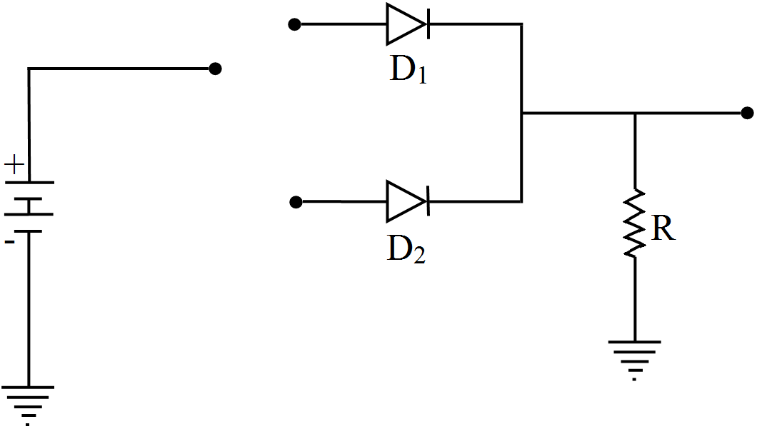
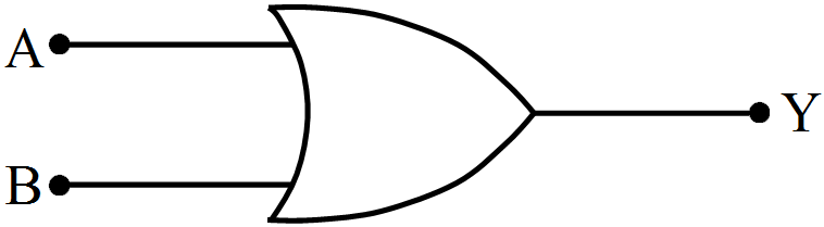
Answer

The logic gate shown in the circuit diagram is OR gate.

Symbol of OR gate:
Input
 
Output
A
B
Y
0
0
1
1
0
1
0
1
1
1
1
1
The gate obtained by combining OR gate with NOT gate will be NOR gate.

Need a full question paper?

Generate a complete, print-ready paper with questions like this in minutes — across 16+ boards, with answer keys.

Start Generating Free

Similar questions

What is the power dissipated by an ideal inductor in ac circuit? Explain.
A straight wire carrying a current of $12 A$ is bent into a semi-circular arc of radius $2.0 cm$ as shown in Fig. 4.11 (a). Consider the magnetic field $B$ at the centre of the arc. (a) What is the magnetic field due to the straight segments? (b) In what way the contribution to $B$ from the semicircle differs from that of a circular loop and in what way does it resemble? (c) Would your answer be different if the wire were bent into a semi-circular arc of the same radius but in the opposite way as shown in Fig. 4.11(b)?
Image
Explain the rules for obtaining image due to reflection from a spherical mirror.
A voltmeter consists of a $25\Omega$ coil connected in series with a $575\Omega$ resistor. The coil takes 10mA for full scale deflection. What maximum potential difference can be measured by this voltmeter?
Describe experiment of relative motion between magnet and coil explaining phenomenon of electromagnetic induction.
Find the maximum kinetic energy of the photoelectrons ejected when light of wavelength 350nm is incident on a cesium surface. Work function of cesium = 1.9eV
Find the equivalent resistance of the network shown in figure. between the points a and b.

Show that the interior of a conductor can have no excess charge in the static situation.
What is meant by radioactive equilibrium?