Gujarat BoardEnglish MediumSTD 12 SciencePhysicsSEMICONDUCTOR ELECTRONICS: MATERIALS, DEVICES AND SIMPLE CIRCUITS3 Marks
Question
Give brief explanation of a semi-conductor diode.
✓
Answer
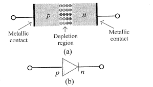
→A semiconductor diode is basically a $p-n$ junction with metallic contacts provided at the ends for the application of an external voltage. It is a two terminal device. A $p-n$ junction diode is symbolically represented as shown in fig. (b). →The direction of arrow indicates the conventional direction of current (When the diode is under forward bias.) The equilibrium barrier potential can be altered by an external voltage V across the diode. →The situation of $p-n$ junction diode under equilibrium (without bias) is shown in fig. (a) and (b).
Need a full question paper?
Generate a complete, print-ready paper with questions like this in minutes — across 16+ boards, with answer keys.