Question types

Semiconductor Electronic: Material, Devices And Simple Circuits question types

478 questions across 7 question groups — pick any mix to generate a Physics paper with step-by-step answer keys.

478
Questions
7
Question groups
5
Question types
Sample Questions

Semiconductor Electronic: Material, Devices And Simple Circuits questions

One sample from each question group in this chapter. Select any group above to see the full set with answer keys.

Q 4M.C.Q [1M]1 Mark
The energy gap between the valence band and the condition band for a material is 6eV. The material is?
  • A
    An insulator
  • B
    A metal
  • C
    An intrinsic semiconductor
  • D
    A superconductor
View full solution
Two statements are given-one labelled Assertion (A) and the other labelled Reason (R). Select the correct answer to these questions from thecodes(a), (b), (c) and (d) as given below.
  1. Both A and R are true and R is the correct explanation of A.
  2. Both A and R are true but R is not the correct explanation of A.
  3. A is true but R is false.
  4. A is false and R is also false.
Assertion: Diode lasers are used as optical sources in optical communicatiod.
Reason: Diode lasers consume less energy.
View full solution
Two statements are given-one labelled Assertion (A) and the other labelled Reason (R). Select the correct answer to these questions from thecodes(a), (b), (c) and (d) as given below.
  1. Both A and R are true and R is the correct explanation of A.
  2. Both A and R are true but R is not the correct explanation of A.
  3. A is true but R is false.
  4. A is false and R is also false.
Assertion: Diamond behaves like an insulator.
Reason: There is a large energy gap between valence band and conduction band of diamond.
View full solution
Two statements are given-one labelled Assertion (A) and the other labelled Reason (R). Select the correct answer to these questions from thecodes(a), (b), (c) and (d) as given below.
  1. Both A and R are true and R is the correct explanation of A.
  2. Both A and R are true but R is not the correct explanation of A.
  3. A is true but R is false.
  4. A is false and R is also false.
Assertion: In a semiconductor diode, the reverse biased current is due to drift of free electrons and holes.
Reason: The drift of electrons and holes is due to thermal excitation.
View full solution
Two statements are given-one labelled Assertion (A) and the other labelled Reason (R). Select the correct answer to these questions from thecodes(a), (b), (c) and (d) as given below.
  1. Both A and R are true and R is the correct explanation of A.
  2. Both A and R are true but R is not the correct explanation of A.
  3. A is true but R is false.
  4. A is false and R is also false.
Assertion: : The half-wave rectifier work only for positive half cycle of ac.
Reason: In half-wave rectifier only one diode is used.
View full solution
Two statements are given-one labelled Assertion (A) and the other labelled Reason (R). Select the correct answer to these questions from thecodes(a), (b), (c) and (d) as given below.
  1. Both A and R are true and R is the correct explanation of A.
  2. Both A and R are true but R is not the correct explanation of A.
  3. A is true but R is false.
  4. A is false and R is also false.
Assertion: The resistance of p-n junction is low when forward biased and is high when reverse biased.
Reason: In reversed biased, the depletion layer is reduced.
View full solution
In an n-type silicon, which of the following statement is true:
  1. Electrons are majority carriers and trivalent atoms are the dopants.
  2. Electrons are minority carriers and pentavalent atoms are the dopants.
  3. Holes are minority carriers and pentavalent atoms are the dopants.
  4. Holes are majority carriers and trivalent atoms are the dopants.
View full solution
In an unbiased p-n junction, holes diffuse from the p-region to n-region because,
  1. Free electrons in the n-region attract them.
  2. They move across the junction by the potential difference.
  3. Hole concentration in p-region is more as compared to n-region.
  4. All the above.
View full solution
Carbon, silicon and germanium have four valence electrons each. These are characterised by valence and conduction bands separated by energy band gap respectively equal to (Eg)C, (Eg)si and (Eg)Ge. Which of the following statements is true?
  1. (Eg)Si < (Eg)Ge < (Eg)C
  2. (Eg)C < (Eg)Ge < (Eg)Si
  3. (Eg)C > (Eg)Si > (Eg)Ge
  4. (Eg)C = (Eg)Si = (Eg)Ge
View full solution
When a forward bias is applied to a p-n junction, it
  1. Raises the potential barrier.
  2. Reduces the majority carrier current to zero.
  3. Lowers the potential barrier.
  4. None of the above.
View full solution
Two amplifiers are connected one after the other in series (cascaded). The first amplifier has a voltage gain of 10 and the second has a voltage gain of 20. If the input signal is 0.01 volt, calculate the output ac signal.
View full solution
Q 213 Marks Question3 Marks
Write the two processes that take place in the formation of a p-n junction. Explain with the help of a diagram, the formation of depletion region and barrier potential in a p-n junction.
View full solution
Q 233 Marks Question3 Marks
The number of silicon atoms per m3 is 5 × 1028. This is doped simultaneously with 5 × 1022 atoms per m3 of Arsenci and 5 × 1020 per m3 atoms of Indium. Calculate the number of electrons and holes Given that ni = 1.5 × 1016 m-3. Is the material n-type or p-type?
View full solution
Q 243 Marks Question3 Marks
Write the truth table for a NAND gate connected as given in Fig. 14.45.

Hence identify the exact logic operation carried out by this circuit.
View full solution
Graph showing the variation of current versus voltage for a material GaAs is shown in the figure. Identify the region of.
  1. Negative resistance.
  2. Where Ohm's law is obeyed.
View full solution
  1. State briefly the processes involved in the formation of p-n junction explaining clearly how the depletion region is formed.
  2. Using the necessary circuit diagrams, show how the V-I characteristics of a p-n junction are obtained in
  1. Forward biasing.
  2. Reverse biasing.

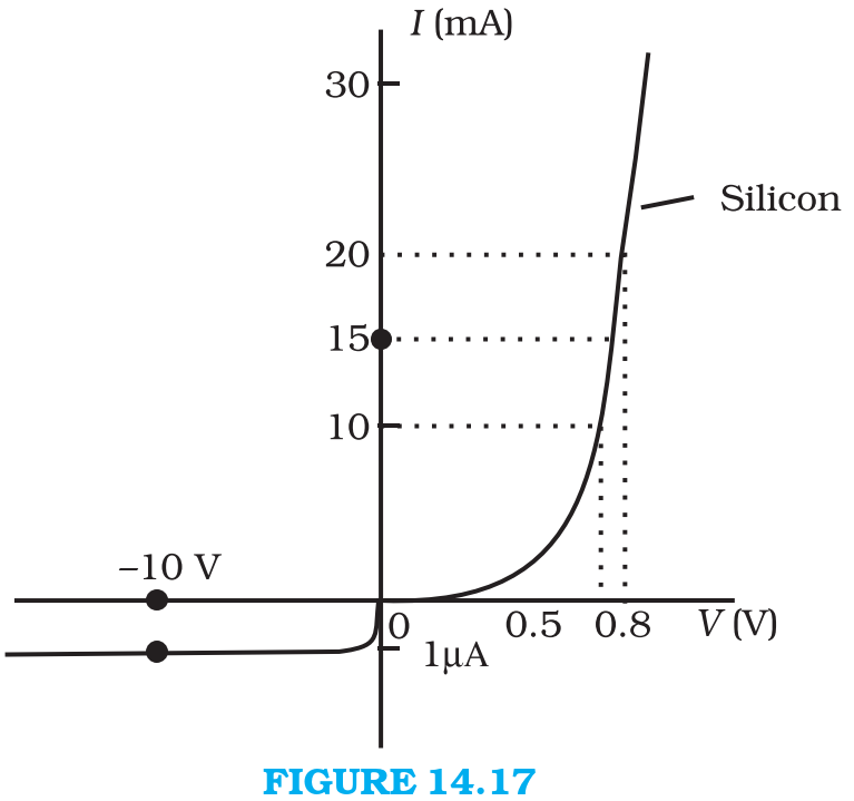
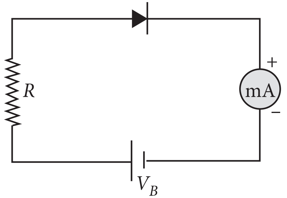
How are these characteristics made use of in rectification?

View full solution
A silicon p-n junction diode is connected to a resistor Rand a battery of voltage VB through milliammeter (mA) as shown in figure. The knee voltage for this junction diode is VN = 0.7V. The p-n junction diode requires a minimum current of 1mA to attain a value higher than the knee point on the I-V characteristics of this junction diode. Assuming that the voltage Vacross the junction is independent of the current above the knee point. A p-n junction is the basic building block of many semiconductordevices like diodes. Important process occurring during the formation of a p-n junction are diffusion and drift. ln an n-type semiconductor concentration of electrons is more as compared to holes. ln a p-type semiconductor concentration of holes is more as compared to electrons.

  1. If V= 5V, the maximum value of R so that the voltage V is above the knee point voltage is:
  1. $40\text{k}\Omega$
  2. $4.3\text{k}\Omega$
  3. $5.0\text{k}\Omega$
  4. $5.7\text{k}\Omega$
  1. If VB = 5V, the value of R in order to establish a current to 6mA in the circuit is:
  1. $833\Omega$
  2. $717\Omega$
  3. $950\Omega$
  4. $733\Omega$
  1. If VB = 6V, the power dissipated in the resistor R, when a current of 6mA flows in the circuit is:
  1. 30.2mW
  2. 30.8mW
  3. 31.2mW
  4. 31.8mW
  1. When the diode is reverse biased with a voltage of 6V and Vbi = 0.63V. Calculate the total potential.
  1. 9.27V
  2. 6.63V
  3. 5.27V
  4. 0.63V
  1. Which of the below mentioned statement is false regarding a p-n junction diode?
  1. Diodes are uncontrolled devices.
  2. Diodes are rectifying devices.
  3. Diodes are unidirectional devices.
  4. Diodes have three terminals.
View full solution
P-n junction is a single crystal of Ge or Si doped in such a manner that one half portion of it acts asp-type semiconductor and other half functions as n-type semiconductor. As soon as a p-n junction is formed, the holes from the p-region diffuse into then-region, and electron from n region diffuse in top-region. This results in the development of V 8 across the junction which opposes the further diffusion of electrons and holes through the junction.
  1. In an unbiased p-n junction electrons diffuse from n-region top-region because:
  1. Holes in p-region attract them.
  2. Electrons travel across the junction due to potential difference.
  3. Electron concentration inn-region is more as compared to that in p-region.
  4. Only electrons move from n top region and not the vice-versa.
  1. Electron hole recombination in p-n junction may lead to emission of:
  1. Light.
  2. Ultraviolet rays.
  3. Sound.
  4. Radioactive rays.
  1. In an unbiased p-n junction:
  1. Potential at pis equal to that at n.
  2. Potential at pis + ve and that at n is - ve.
  3. Potential at pis more than that at n.
  4. Potential at pis less than that at n.
  1. The potential of depletion layer is due to:
  1. Electrons.
  2. Holes.
  3. Ions.
  4. Forbidden band.
  1. In the depletion layer of unbiased p-n junction,
  1. It is devoid of charge carriers.
  2. Has only electrons.
  3. Has only holes.
  4. P-n junction has a weak electric field.
View full solution
The electron mobility characterises how quickly an electron can move through a metal of semiconductor when pulled by an electric field. There is an analogous quality for holes, called hole mobility. A block of pure silicon at 300K has a length of 10cm and an area of 1.0cm2. A battery of emf 2V is connected across it. The mobility of electron is 0.14m2 V-1s-1 and their number density is 1.5 × 1016m-3. The mobility of holes is 0.05m2 V-1s-1.
  1. The electron current is:
  1. 6.72 × 10-4A
  2. 6.72 × 10-5A
  3. 6.72 × 10-6A
  4. 6.72 × 10⁻⁷A
  1. The hole current is:
  1. 2.0 × 10-7A
  2. 2.2 × 10-7A
  3. 2.4 × 10-7A
  4. 2.6 × 10-7A
  1. The number density of donor atoms which are to be added up to pure silicon semiconductor to produce an n-type semiconductor of conductivity $6.4\Omega^{-1}\text{cm}^{-1}$ is approximately (neglect the contribution of holes to conductivity).
  1. 3 × 1022m-3
  2. 3 × 1023m-3
  3. 3 × 1024m-3
  4. 3 × 1021m-3
  1. When the given silicon semiconductor is doped with indium, the hole concentration increases to 4.5 × 1023m-3. The electron concentration in doped silicon is:
  1. 3 × 109m-3
  2. 4 × 109m-3
  3. 5 × 109m-3
  4. 6 × 109m-3
  1. Pick out the statement which is not correct.
  1. At a low temperature, the resistance of a semiconductor is very high.
  2. Movement of holes is restricted to the valence band only.
  3. Width of the depletion region increases as the forward bias voltage increases in case of a p-n junction diode.
  4. ln a forward bias condition, the diode heavily conducts.
View full solution
In a p-n junction diode, the current I can be expressed as,
$I=I_0\ \text{exp}\Big(\frac{\text{eV}}{2\text{k}_{\text{B}}\text{T}}-1\Big)$
where $I_0$ is called the reverse saturation current, V is the voltage across the diode and is positive for forward bias and negative for reverse bias, and $I$ is the current through the diode, kg is the Boltzmann constant (8.6×10⁻⁵ eV/K) and T is the absolute temperature. If for a given diode $I_0$ = 5×10-12 A and T = 300 K, then,
  1. What will be the forward current at a forward voltage of 0.6V?
  2. What will be the increase in the current if the voltage across the diode is increased to 0.7V?
  3. What is the dynamic resistance?
  4. What will be the current if reverse bias voltage changes from 1V to 2V?
View full solution
In an intrinsic semiconductor the energy gap Eg is 1.2eV. Its hole mobility is much smaller than electron mobility and independent of temperature. What is the ratio between conductivity at 600K and that at 300K? Assume that the temperature dependence of intrinsic carrier concentration ni is given by,
$\text{n}_{\text{i}}=\text{n}_{\text{0}}\ {\text{exp}}\Big(-\frac{\text{E}_\text{g}}{2{\text{K}_{\text{B}}}{\text{T}}}\Big)$
where n0 is a constant.
View full solution
  1. Describe briefly, with the help of a diagram, the role of the two important processes involved in the formation of a p-n junction.
  2. Name the device which is used as a voltage regulator. Draw the necessary circuit diagram and explain its working.
View full solution
  1. Draw the circuit diagrams of a p-n junction diode in (i) forward bias, (ii) reverse bias. How are these circuits used to study the V - I characteristics of a silicon diode? Draw the typical V - I characteristics.
  2. What is a light emitting diode (LED)? Mention two important advantages of LEDs over conventional lamps.
View full solution

Generate a Semiconductor Electronic: Material, Devices And Simple Circuits paper free

Pick question groups from the list above, set marks and difficulty, and export a branded PDF with step-by-step answer keys. First 3 chapters free — no signup.

Download App