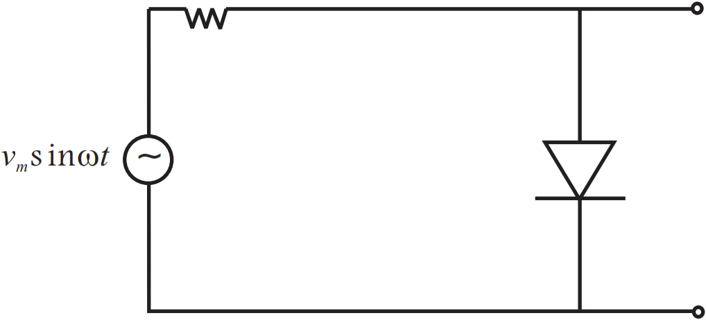
Questions · Page 2 of 5

M.C.Q (1 Marks)

MCQ 511 Mark
Hole is:
  • A
    An anti$-$particle of electron.
  • A vacancy created when an electron leaves a covalent bond.
  • C
    Absence of free electrons.
  • D
    An artifically created particle.
Answer
Correct option: B.
A vacancy created when an electron leaves a covalent bond.

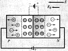
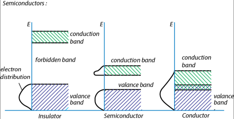
Concept of holes in the semiconductor:
When an electron is removed from a covalent bond, it leaves a vacancy behind. An electron from a neighbouring atom can move into this vacancy, leaving the neighbour with a vacancy. In this way the vacancy formed is called a hole $($or cotter$)$, and can travel through the material and serve as an additional current carriers.
A hole is considered as a seat of positive charge, having magnitude of charge equal to that of an electron.
Holes acts as a virtual charge, although there is no physical charge on it.
Effective mass of hole is more than an electron.
Mobility of hole is less than an electron.

View full question & answer
MCQ 521 Mark
The output of $OR$ gate is $1:$
  • If either one or both inputs are $1$
  • B
    Only if both inputs are $1$
  • C
    If either input is zero
  • D
    If both inputs are zero
Answer
Correct option: A.
If either one or both inputs are $1$

At least one input required to activate or $−$ gate

View full question & answer
MCQ 531 Mark
A $p-$type semiconductor is:
  • A
    Positively charged.
  • B
    Negatively charged.
  • Uncharged.
  • D
    Uncharged at $0K$ but charged at higher ternperatures.
Answer
Correct option: C.
Uncharged.

A $p-$type semiconductor is formed by doping a pure semiconductor with a $p-$type material. As impurity atoms take the position of the germanium atom in a germanium crystal, three electrons of a $p-$type material form covalent bonds by sharing electrons with three neighbouring germanium atoms. However, the fourth covalent bond is left incomplete, with a want of one electron. This creates a hole. As the atom as a whole is neutral, the $p-$type material is also neutral.

View full question & answer
MCQ 541 Mark
The breakdown in a reverse biased $p-n$ junction diode is more likely to occur due to:
  • A
    Large velocity of the minority charge carriers if the doping concentration is small.
  • B
    Large velocity of the minority charge carriers if the doping concentration is large.
  • C
    Strong electric field in the depletion region if the doping concentration is large.
  • $A$ and $C$ both
Answer
Correct option: D.
$A$ and $C$ both
Solution:
Reverse biasing: Positive terminal of the battery is connected to the $N-$crystal and negative terminal of the battery is connected to $P-$crystal.
  1. In reverse biasing width of depletion layer increases
  2. In reverse biasing resistance offered $R_{\text {Reverse }}=10^5 \Omega$.
  3. Reverse bias supports the potential barrier and no current flows across the junction due to the diffusion of the majority carriers.
$($A very small reverse current may exist in the circuit due to the drifting of minority carriers across the junction$)$
  1. Break down voltage: Reverse voltage at which break down of semiconductor occurs. For Ge it is $25V$ and for $Si$ it is $35V.$

So, we conclude that in reverse biasing, ionization takes place because the minority charge carriers will be accelerated due to reverse biasing and striking with atoms which in turn cause secondary electrons and thus more number of charge carriers.
When doping concentration is large, there will be a large number of ions in the depletion region, which will give rise to a strong electric field.
View full question & answer
MCQ 551 Mark
The leakage current across a pn junction is due to $........$
  • Minority carriers
  • B
    Majority carriers
  • C
    Junction capacitance
  • D
    None of these
Answer
Correct option: A.
Minority carriers

When a diode is reverse biased, its depletion region increases in width. Thus depletion region would correspond to an insulator. However still some current actually flows through the depletion region. This is due to the pushing of minority carriers across the depletion region causing very small reverse 'leakage current'.

View full question & answer
MCQ 561 Mark
In Fig., assuming the diodes to be ideal:
  • A
    $D_1$ is forward biased and $D_2$ is reverse biased and hence current flows from $A$ to $B$.
  • $D_2$ is forward biased and $D_1$ is reverse biased and hence no current flows from $B$ to $A$ and vice versa.
  • C
    $D_1$ and $D_2$ are both forward biased and hence current flows from $A$ to $B.$
  • D
    $D_1$ and $D_2$ are both reverse biased and hence no current flows from $A$ to $B$ and vice versa.
Answer
Correct option: B.
$D_2$ is forward biased and $D_1$ is reverse biased and hence no current flows from $B$ to $A$ and vice versa.

A symbol of the diode is represented like this: In this problem first we have to check the polarity of the diodes. $-10$ is the lower voltage in the circuit. Now $p-$side of $p-n$ juction $D_1$ is connected to lower voltage and $n-$side of $D_1$ to higher voltage. Thus $D_1$ is reverse biased. Now, let us analyse $2^{\text {nd }}$ diode of the given circuit. The $p$-side of $p-n$ junction $D_1$ is at higher potential and $n$-side of $D_2$ is at lower potential. Therefore $D_2$ is forward biased.

Hence, current flows through the jucntion from $B$ to $A.$

View full question & answer
MCQ 571 Mark
In insulator:
  • A
    Valence band is partially filled with electrons.
  • B
    Conduction band is partially filled with electrons.
  • C
    Conduction band is filled with electrons and valence band is empty.
  • Conduction band is empty and valence band is filled with electrons.
Answer
Correct option: D.
Conduction band is empty and valence band is filled with electrons.

Insulators are the materials which do not conduct electricity. All the electrons are filled in valance band whereas the conduction band is empty. Moreover, the energy band gap in insulators is very large, thus electrons cannot jump from valence band to conduction band.

View full question & answer
MCQ 581 Mark
In intrinsic semiconductors:
  • A
    $n > p$
  • B
    $p > n$
  • $n = p$
  • D
    $n = 0$
Answer
Correct option: C.
$n = p$

Intrinsic semiconductors are pure ones. Hence there is no question of impurity. Valence band is the range of energy of electrons which are in the valence shell of the atoms of a substance. Conduction band is the range of energy of electrons which are free and available for conduction.
At room temperature, some electrons of intrinsic semiconductors get excited and reach the conduction band. During this process, the electrons leave empty spaces in the valence shell. These empty spaces are known as holes in a semiconductor. Number of free electrons $(n)$ is equal to the number of holes $(p).$

View full question & answer
MCQ 591 Mark
Given above are four logic gate symbols. Those for $\text{OR, NOR}$ and $\text{NAND}$ are respectively:
  • A
    $\text{a, d, c}$
  • B
    $\text{d, a, b}$
  • $\text{a, c, d}$
  • D
    $\text{d, b, a}$
Answer
Correct option: C.
$\text{a, c, d}$

$a-$ represent $\text{OR}$ gate
$b-$ represent the $\text{AND}$ gate
$c-$ represent, the combination of $\text{OR}$ and $\text{NOT}$ gate, $\text{NOR}$ gate.
$d-$ represent, the combination of $\text{AND}$ and $\text{NOT}$ gate, $\text{NAND}$ gate.

View full question & answer
MCQ 601 Mark
Statement $-1: \text{NAND}$ and $\text{NOR}$ gates are called digital building blocks.
Statement$-2:$ The repeated use of $\text{NAND} ($or $\text{NOR})$ gates can produce all the basis or complicated gates.
  • A
    Statement $-1$ is false, Statement $-2$ is true.
  • Statement $1-$is true, Statement $-2$ is true and Statement $-2$ is correct explanation of Statement$-1.$
  • C
    Statement $1-$is true, Statement $-2$ is true and statement $-2$ is not correct explanation of statement$-1.$
  • D
    Statement $1-$is true, Statement $-2$ is false.
Answer
Correct option: B.
Statement $1-$is true, Statement $-2$ is true and Statement $-2$ is correct explanation of Statement$-1.$
$\text{NAND}$ or $\text{NOR}$ gates are called universal gates or digital building blocks. Also, the repeated use of $\text{NAND} ($or $\text{NOR)}$ gates can produce all the basis or any complicated gates can be formed using $\text{NAND} ($or $\text{NOR)}$ gates. Hence, statement $1-$is true statement $-2$ is true statement $-2$ is correct explanation of statement$-1$.
View full question & answer
MCQ 611 Mark
If the two ends of a $p-n$ junction are joined by a wire:
  • There will not be a steady current in the circuit.
  • B
    There will be a steady current from the n-side to the $p-$side.
  • C
    There 'will a steady current from the $p-$side. to the $n-$side.
  • D
    There may or may not be a current depending upon the resistance of the connecting wire.
Answer
Correct option: A.
There will not be a steady current in the circuit.

In a $p‒n$ junction, current flows only if it is connected to the battery. If two ends of a $p‒n$ junction are joined by a wire, then there will be diffusion and drift currents in the circuit and they will cancel each other. Hence, no current will flow in the circuit.

View full question & answer
MCQ 621 Mark
In a semiconductor diode, the barrier potential offers opposition to:
  • A
    Holes in $P-$region only.
  • B
    Free electrons in $N-$region only.
  • Majority carriers in both regions.
  • D
    Majority as well as minority carriers in both regions.
Answer
Correct option: C.
Majority carriers in both regions.
View full question & answer
MCQ 631 Mark
A semiconductor device is connected in a series circuit with a battery and resistance. A current is found to pass through the circuit. If the polarity of the battery is reversed, the current drops almost to zero. The device may be:
  • A
    A $p-$type semiconductor
  • B
    An $n-$type semiconductor
  • A $p-n$ junction
  • D
    An intrinsic semiconductor
Answer
Correct option: C.
A $p-n$ junction

An ideal diode acts like an open switch when rivers biased and like a closed switch when forward biased.

View full question & answer
MCQ 641 Mark
In a metal, the separation between conduction band and valence band is of the order:
  • A
    $100\ eV$
  • B
    $10\ eV$
  • $0\ eV$
  • D
    $1\ eV$
Answer
Correct option: C.
$0\ eV$
Energy band gap is the energy difference between conduction band and valence band, i. e., energy required to an electron to overcome the energy levels between conduction band and valence band. In conductors, electrons are loosely bound to the nucleus hence, can detach easily at room temperature also.
A large number of free electrons thus, available are conduction electrons. The energy level of these electrons corresponds to the conduction level, hence valance level and conduction level are overlapped. Due to this, there is no gap between conduction band and valence band hence, for metals their separation is of the order of $0\ eV.$
View full question & answer
MCQ 651 Mark
In the depletion region of a diode:
  • A
    There are no mobile charges.
  • B
    Equal number of holes and electrons exist, making the region neutral.
  • C
    Immobile charged ions exist.
  • All of the above.
Answer
Correct option: D.
All of the above.
Solution:
On account of difference in concentration of charge carrier in the two sections of P-N junction, the electrons from N-rcgion diffuse through the junction into P-region and the hole from P-region diffuse into N-region.

Due to diffusion, neutrality of both N-and P-type semiconductor is disturbed, a layer of negative charged ions appear near the junction in the P-crystal and a layer of positive ions appears near the junction in N-crystal. This layer is called depletion layer.
The thickness of depletion layer is 1 micron = $10^{-6}$m.
Width of depletion layer ∞ 1/Dopping
Depletion is directly proportional to temperature.
Important point: The P-N junction diode is equivalent to capacitor in which the depletion layer acts as a dielectric.
View full question & answer
MCQ 661 Mark
Statement$-1: \text{NOT}$ gate is also called invertor circuit.Statement$-2: \text{NOT}$ gate inverts the input order.
  • A
    Statement $-1$ is false, statement $-2$ is true.
  • Statement $-1$is true, statement $-2$ is true and statement $-2$ is correct explanation of statement$-1.$
  • C
    Statement $-1$ is true, statement $-2$ is true but statement $-2$ is not correct explanation of statement$-1.$
  • D
    Statement $-1$ is true, statement $-2$ is false.
Answer
Correct option: B.
Statement $-1$is true, statement $-2$ is true and statement $-2$ is correct explanation of statement$-1.$

$\text{NOT}$ gate is also called invertor circuit since $\text{NOT}$ gate inverts the input order. Hence, statement $-1$ is true statement$-2$ is true statement$-2$ is correct explanation of statement$-1.$

View full question & answer
MCQ 671 Mark
The $n-$side of the depletion layer of a $p-n$ junction.
  • A
    Always has same width as of the $p-$side
  • B
    Has no bound charges
  • C
    Is negatively charged
  • Is positively charged
Answer
Correct option: D.
Is positively charged
The diffusion of electrons from n side to $p$ side makes the n side of the depletion layer of pn junction positively charged since it becomes deficient in electrons and each side was neutral in the beginning.
View full question & answer
MCQ 681 Mark
If the bandgap between valence band and conduction band in a material is $0\ eV$, then the material is:
  • A
    Semiconductor
  • Good conductor
  • C
    Superconductor
  • D
    Insulator
Answer
Correct option: B.
Good conductor

In good conductors, the valance band and the conduction band overlap each other resulting in a zero band gap energy. Whereas, bandgap in insulator is nearly $5\ eV$ and that in semiconductors is nearly $1.1\ eV.$
Hence the given material is a good conductor.

View full question & answer
MCQ 691 Mark
In insulators $........ (C.B$ is conduction band and $V.B$ is valence band$)$
  • A
    $V.B.$ is partially filled with electrons.
  • B
    $C.B.$ is partially filled with electrons.
  • $C.B.$ is empty and $V.B.$ is filled with electrons.
  • D
    $C.B$. is filled with electrons and $V.B.$ is empty.
Answer
Correct option: C.
$C.B.$ is empty and $V.B.$ is filled with electrons.
As shown in the image, insulators have a very large forbidden gap. Their conduction band is empty, thus they cannot conduct electricity under normal room temperature and pressure conditions. The valence band is full.
View full question & answer
MCQ 701 Mark
In which of the following statements, the obtained impure semiconductor is of $p-$type?
  • A
    Germanium is doped with bismuth.
  • B
    Silicon is doped with antimony.
  • Germanium is doped with gallium.
  • D
    Silicon is doped with phosphorus.
Answer
Correct option: C.
Germanium is doped with gallium.

A p-type semiconductor is produced by doping a $14$ group element with a $13$ group element as $14$ group element has $4$ valence electron whereas that of group $13$ has $3$ valence electron. We know that Germanium is a $14$ group element and gallium is a $13$ group element, thus doping germanium with gallium forms a $p-$type semiconductor.

View full question & answer
MCQ 711 Mark
The conduction band and valency band of a good conductor are:
  • A
    Well separated.
  • B
    Just touch.
  • C
    Very close.
  • Overlapped.
Answer
Correct option: D.
Overlapped.

In conductors, electrons are loosely bound to the nucleus hence, can detach easily at room temperature also. A large number of free electrons thus, available are conduction electrons.
The energy level of these electrons corresponds to the conduction level, hence valance level and conduction level are overlapped.

View full question & answer
MCQ 721 Mark
Semiconductors are generally made up of which substance?
  • Silicon
  • B
    Carbon
  • C
    Phosphorus
  • D
    Boron
Answer
Correct option: A.
Silicon

Semiconductors are made of Si, generally. Because $Si$ is the second most abundant element in earth's crust after oxygen and is less expensive than other semiconductors used in intrinsic semiconductors.

View full question & answer
MCQ 731 Mark
$\text{NAND}$ and $\text{NOR}$ gates are called universal gates primarily because they:
  • A
    Are available universally.
  • Can be combined to produce $\text{OR, AND}$ and $\text{NOT}$ gates.
  • C
    Are widely used in Integrated circuit packages.
  • D
    Are easiest to manufacture.
Answer
Correct option: B.
Can be combined to produce $\text{OR, AND}$ and $\text{NOT}$ gates.
View full question & answer
MCQ 741 Mark
In an insulator, the energy gap between conduction band and valence band is about:
  • A
    $0\ eV$
  • $6\ eV$
  • C
    $1\ eV$
  • D
    $0.6\ eV$
Answer
Correct option: B.
$6\ eV$

Atoms are neutral in the insulator, thus there are no valence electrons in the outer orbit. The electrons are tightly bound with the nucleus hence, at room temperature thermal energy is not enough to push the electrons into conduction band and hence, no electrons are available for conduction.
The energy required for electron to escape out from orbit and to over come the energy gap is thus of the order of $6\ eV.$

View full question & answer
MCQ 751 Mark
Which of the following are correct for insulators?
  • A
    The valence band is partially filled with electrons.
  • B
    The conduction band is partially filled with electrons.
  • C
    The conduction band is partially filled with electrons and valence band is empty.
  • The conduction band is empty and the valence band is filled with electrons.
Answer
Correct option: D.
The conduction band is empty and the valence band is filled with electrons.

In insulators, the electrons are very tightly bound to the nucleus. At a room temperature, thermal energy is not enough to push electrons into conduction band. The energy band gap is very high. Thus the conduction band is empty and the valence band is filled with electrons.

View full question & answer
MCQ 761 Mark
The concepts of holes is introduced based on:
  • The notion that it is a whole lot easier to keep track of the missing particles in an "almost$-$full" band.
  • B
    The keeping track of the actual electrons in that band.
  • C
    The charge of holes
  • D
    None of the above
Answer
Correct option: A.
The notion that it is a whole lot easier to keep track of the missing particles in an "almost$-$full" band.

The concept of holes was introduced so as to occupy the empty spaces left by the missing electron. For example, in a valence band, when an electron jumps from valence to conduction band, an empty space is created in valence band which is occupied by a hole.

View full question & answer
MCQ 771 Mark
In a semiconductor, the forbidden energy gap between the valence band and the conduction band is of the order is:
  • A
    $1\ MeV.$
  • B
    $0.1\ Mev.$
  • $1\ eV.$
  • D
    $5\ eV.$
Answer
Correct option: C.
$1\ eV.$
View full question & answer
MCQ 781 Mark
Forbidden gap in a pure conductor is:
  • $0\ eV$
  • B
    $0.7\ eV$
  • C
    $1.1\ eV$
  • D
    $6\ eV$
Answer
Correct option: A.
$0\ eV$

Forbidden band gap is the group of energy levels that cannot be occupied by the electrons, these energies lies in between conduction band and valence band. In pure conductors, electrons are loosely bound to the nucleus hence, can detach easily at room temperature also.
A large number of free electrons thus, available are conduction electrons. The energy level of these electrons corresponds to the conduction level, hence valence level and conduction level are overlapped.
Due to this, there is no forbidden band gap present in between conduction band and valence band hence, for metals the forbidden band gap is $0\ eV.$

View full question & answer
MCQ 791 Mark
The forbidden energy gap for germanium crystal at $0 K$ is:
  • A
    $0.071\ eV.$
  • $0.71\ eV.$
  • C
    $2.57\ eV.$
  • D
    $6.57\ eV.$
Answer
Correct option: B.
$0.71\ eV.$
View full question & answer
MCQ 801 Mark
Which of the following statement$(s)$ is/are true about holes?
  • They flow from positive terminal to negative terminal.
  • B
    They flow from negative terminal to positive terminal.
  • C
    They do not flow
  • D
    None of these
Answer
Correct option: A.
They flow from positive terminal to negative terminal.
Electrons flow from negative to positive terminal of battery. whenever the electric current flows from positive terminal of battery to negative terminal of battery is called conventional current. the conventional current has same direction of flow of holes but opposite to direction of flow of from electron.
View full question & answer
MCQ 811 Mark
The output of the given circuit in Fig.
  • A
    Would be zero at all times.
  • B
    Would be like a half wave rectifier with positive cycles in output.
  • Would be like a half wave rectifier with negative cycles in output.
  • D
    Would be like that of a full wave rectifier.
Answer
Correct option: C.
Would be like a half wave rectifier with negative cycles in output.
Key Concept:
  1. During positive half cycle,
Diode $\rightarrow $ Forward biased
Output signal $\rightarrow $ obtained
  1. During negative half cycle,
Diode $\rightarrow $ reverse biased
Output signal $\rightarrow $ not obtained
  1. Output voltage is obtained across the load resistance $RL$. It is not constant but pulsating $($mixture of $ac$ and $dc)$ in nature.
  2. Average output in one cycle
  3. $\text{r.m.s.}$ output: $\text{I}_\text{rms}=\frac{\text{I}_0}{2},\text{V}_\text{rms}=\frac{\text{V}_0}{2}$
When the diode is forward biased during positive half cycle of input $AC$ voltage, the resistance of $p-n$ junction is low. The current in the circuit is maximum. In this situation, a maximum potential difference will appear across resistance connected in a series of circuit. This result into zero output voltage across $p-n$ junction.
And when the diode is reverse biased during negative half cycle of $AC$ voltage, the $p-n$ junction is reverse biased. The resistance of $p-n$ junction becomes high which will be more than resistance in series. That is why, there will be voltage across $p-n$ junction with negative cycle in output, hence option $(c)$ is correct.
View full question & answer
MCQ 821 Mark
The transistor are usually made of:
  • Metal oxides with high temperature coefficient of resistivity.
  • B
    Metals with high temperature coefficient of resistivity.
  • C
    Metals with low temperature coefficient of resistivity.
  • D
    Semiconducting materials having low temperature coefficient of resistivity.
Answer
Correct option: A.
Metal oxides with high temperature coefficient of resistivity.
View full question & answer
MCQ 831 Mark
The bond, that exists in a semiconductor is:
  • Covalent bond
  • B
    Ionic bond
  • C
    Metalic bond
  • D
    Hydrogen bond
Answer
Correct option: A.
Covalent bond

Semi$-$conductors are made of $14^{th}$ Group elements which form covalent bonding.

View full question & answer
MCQ 841 Mark
The impurity atoms with which pure silicon may be doped to make it a $p-$type semiconductor are those of:
  • A
    Phosphorus.
  • Boron.
  • C
    Antimony.
  • D
    Nitrogen.
Answer
Correct option: B.
Boron.
View full question & answer
MCQ 851 Mark
A $p-n$ junction diode cannot be used:
  • A
    As a rectifier.
  • B
    For converting light energy to electric energy.
  • C
    For getting light radiation.
  • For increasing the amplitude of an $AC$ signal
Answer
Correct option: D.
For increasing the amplitude of an $AC$ signal

To increase the amplitude of an $\text{AC}$ signal, transistors are used. $p-n$ junction diodes can be used as rectifiers and in photo$-$diode and $\text{LED.}$

View full question & answer
MCQ 861 Mark
To get an output $Y=1$ from the circuit above, the input must be:
  • A
    $A-0, B-1, C-0$
  • B
    $A-1, B-0, C-0$
  • $A-1, B-0, C-1$
  • D
    $A-1, B-1, C-0$
Answer
Correct option: C.
$A-1, B-0, C-1$
Logic gate $OR$ is used for addition of the input signals and Logic gate $\text{AND}$ is used for multiplication of the input signals. Hence, here inputs $A = 1, B = 0$ and $C = 1$ will yield the output $Y = 1.$
View full question & answer
MCQ 871 Mark
A hole diffuses from the $p-$side to the $n-$side in a $p-n$ junction. This means that.
  • A
    A bond ia broken on the $n-$side and the electron freed from the bond jumps to the conduction band.
  • B
    A conduction electron on the $p-$side jumps to a broken bond to complete it.
  • A bond is broken on the $n-$side and the electron freed from the bond jumps to a broken bond on the $p-$side to complete it.
  • D
    A bond is broken on the $p-$side and the electron freed from the bond jumps to a broken bond on the $n-$side to complete it.
Answer
Correct option: C.
A bond is broken on the $n-$side and the electron freed from the bond jumps to a broken bond on the $p-$side to complete it.
A hole diffuses from the $p$ side to the n side in a $p−n$ junction; that is, an electron moves from the n side to the $p$ side. This implies that a bond is broken on the $n$ side. As the electron travels towards the $p$ side, which is rich in holes, it combines with a hole. A hole is created because of the deficiency of one electron. So, when an electron combines with a hole, it completes that bond.
View full question & answer
MCQ 881 Mark
In the Boolean algebra, the following one is wrong :
  • A
    $1 + 0 = 1$
  • B
    $0 + 1 = 1$
  • C
    $1 + 1 = 1$
  • $0 + 0 = 1$
Answer
Correct option: D.
$0 + 0 = 1$
In the Boolean algebra, binary addition is given as :
$1 + 0 = 1$
$0 + 1= 1$
$1 + 1 = 1$
Hence, $0 + 0 =1$ is wrong.
View full question & answer
MCQ 891 Mark
In the Boolean algebra, the following one is wrong:
  • A
    $1.0 = 0$
  • B
    $0.1 = 0$
  • $1.1 = 0$
  • D
    $1.1 = 1$
Answer
Correct option: C.
$1.1 = 0$
In the Boolean algebra,
$1.0 = 0$
$0.1 = 0$
$1.1 = 1$
View full question & answer
MCQ 901 Mark
The cause of the potential barrier in a $p-n$ diode is:
  • A
    Depletion of positive charges near the junction.
  • B
    Concentration of positive charges near the junction.
  • C
    Depletion of negative charges near the junction.
  • Concentration of positive and negative charges near the junction.
Answer
Correct option: D.
Concentration of positive and negative charges near the junction.
During the formation of a junction diode, holes from $p-$ region diffuse into $n-$region and electrons from $n-$region diffuse into $p-$region.
In both cases, when an electrons meets a hole, they cancel the effect at each other and as a result, a thin layer at the junction becomes free from any of charges carriers. This is called depletion layer.
There is a potential gradient in the depletion layer, negative on the $p-$side, and positive on the $n-$side.
The potential difference thus developed across the junction is called potential barrier.
View full question & answer
MCQ 911 Mark
The load voltage is approximately constant when a zener diode is:
  • A
    Forward$-$biased
  • B
    Reverse$-$biased
  • Operating in the breakdown region
  • D
    Unbiased
Answer
Correct option: C.
Operating in the breakdown region
The zener voltage will be a constant only when it is operating in the breakdown region.
View full question & answer
MCQ 921 Mark
The energy band gap is maximum in:
  • A
    Metals
  • B
    Super conductors
  • Insulators
  • D
    Semiconductors
Answer
Correct option: C.
Insulators
In insulators, the electrons are tightly bound with the nucleus hence, at room temperature thermal energy is not enough to push the electrons into conduction band and hence, no electrons are available for conduction.
The energy required for electron to escape out from orbit and to over come the energy gap is thus of the order of $6 eV$, while for semiconductors and conductors it is $($of the order of$) 1\  eV$ and $0$ respectively.
View full question & answer
MCQ 931 Mark
The breakdown in a reverse biased $p-n$ junction diode is more likely to occur due to.
  • Large velocity of the minority charge if the doping concentration is small.
  • B
    Large velocity of the minority charge carriers if the doping concentration is small.
  • C
    Strong electric field in a depletion region if the doping concentration is small.
  • D
    Strong electric filed in the deplention region if the doping conentration is large.
Answer
Correct option: A.
Large velocity of the minority charge if the doping concentration is small.
When it comes to he breakdown in a reverse biased $PN$ junction diode, it will probably happen only because of the accumulation of the higher charge at the biased region and large velocity of the minority charge if the doping concentration is small. This is the main cause the breakdown.
View full question & answer
MCQ 941 Mark
Identify the logic gate in figure.
  • A
    $\text{NAND}$
  • $\text{NOR}$
  • C
    $\text{NOT}$
  • D
    $\text{AND}$
Answer
Correct option: B.
$\text{NOR}$
The symbol of circle shown in figure with $OR$ gate indicates the $\text{NOT}$ gate hence, given gate is $\text{NOR}$ gate.
View full question & answer
MCQ 951 Mark
In $p-$type semiconductors, holes are:
  • Majority carriers
  • B
    Minority carriers
  • C
    Absent
  • D
    None of the above
Answer
Correct option: A.
Majority carriers
$P-$type semiconductors are those which have a $p-$type impurity. A $p-$type impurity is a material in which the atoms have only $3$ Valence Electrons. When they are added to a pure semiconductor, each atom gets bonded with $3$ of atoms of the semiconductor. Between the $4^{th}$ atom of the semiconductor and the atom of the impurity, there is an empty space due to lack of an electron. This empty space is known as a hole. Because of a large existence of $P-$type material in a $p-$type semiconductor, it has more holes as compared to free electrons. Hence holes are majority carriers.
View full question & answer
MCQ 961 Mark
The distinction between conductors, insulators and semiconductors is largely concerned with :
  • A
    Their ability to conduct current
  • B
    The type of crystal lattice
  • C
    Binding energy of their electrons
  • Relative widths of their energy gaps
Answer
Correct option: D.
Relative widths of their energy gaps
According to band theory, distinction between conductors, insulators and semiconductors is based on relative width of energy gaps between valence band and conduction band.
View full question & answer
MCQ 971 Mark
Truth table for the given circuit (Fig.) is:
  • A
  • B
  • D
Answer
Correct option: C.


Solution:

Here, C = A.B and D = Ā.B

E = C + D = (A B) + (Ā .B)

Explanation The truth table of this arrangement of gates can be given
A B Ā C = A.B d = Ā.B E = (C + D)
0 0 1 0 0 0
0 1 1 0 1 1
1 0 0 0 0 0
1 1 0 1 0 0
View full question & answer
MCQ 981 Mark
The drift current in a $p-n$ junction is from the:
  • $N-$side to the $p-$side.
  • B
    $P-$side to the $n-$side.
  • C
    $N-$side to the $p-$side if the junction is forward$-$biased and in the opposite direction if it is reverse biased.
  • D
    $P-$side to the $n-$side if the junction is forward$-$biased and in the opposite direction if it is reverse$-$biased.
Answer
Correct option: A.
$N-$side to the $p-$side.
View full question & answer
MCQ 991 Mark
Electric current is due to drift of electrons in:
  • Metallic conductors
  • B
    Semiconductors
  • C
    Both $(a)$ and $(b)$ above
  • D
    None of the above
Answer
Correct option: A.
Metallic conductors
When an electric field is applied across the metallic conductors the randomly moving electrons are subjected to electrical forces along the direction of the field. Due to this field, the electrons do not give up their randomness of motion, but they will be shifting towards higher potential. That means the electrons will drift towards higher potential along with their random motions.
In semiconductors, in addition to electrons, the travelling vacancies in the valence$-$band electron population $($called 'holes'$)$, act as mobile positive charges and are treated as charge carriers. Electrons and holes are the charge carriers in semiconductors.
Hence, electric current is due to drift of electrons in metallic conductors.
View full question & answer
MCQ 1001 Mark
The energy gap in a conductor at room temperature is $.........$ .
  • A
    Greater than that in a semiconductor.
  • Less than that in a insulator.
  • C
    Greater than that in a insulator.
  • D
    Both $(a)$ and $(b)$ are true.
Answer
Correct option: B.
Less than that in a insulator.
The energy band gap is the energy difference between $2$ bands i.e. valence band and the conduction band. In case of conductors, energy band gap is very small almost overlapping whereas, in case of insulators, the band gap is $∼6 eV$. So. band gap of conductors is less than insulators.

View full question & answer
M.C.Q (1 Marks) - Page 2 - Physics STD 12 Science Questions - Vidyadip