Questions · Page 3 of 5

M.C.Q (1 Marks)

MCQ 1011 Mark
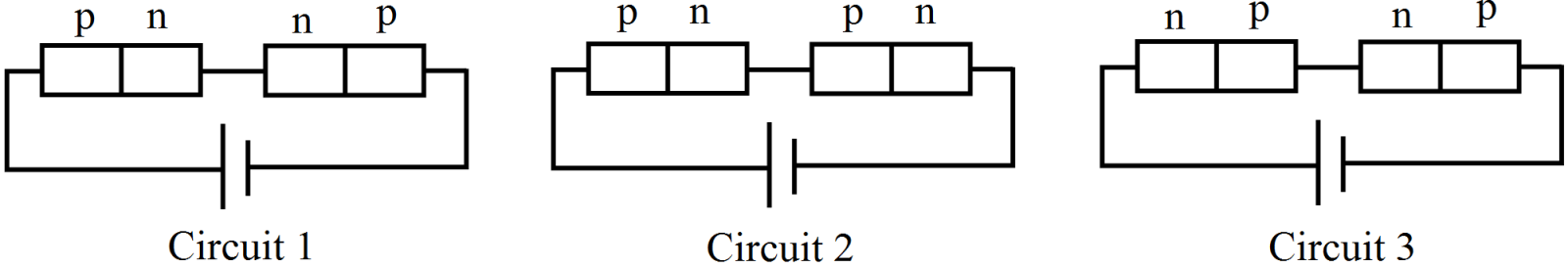
Two identical $p-ri$ junctions may be connected in series with a battery in three ways $($figure$)$. The potential difference across the two $p-n$. junctions are equal in:
  • A
    Circuit $1$ and circuit $2.$
  • Circuit $2$ and circuit $3$.
  • C
    Circuit $3$ and circuit $1.$
  • D
    Circuit $1$ only.
Answer
Correct option: B.
Circuit $2$ and circuit $3$.
In circuit $1$, one diode is forward biassed and the other diode is reverse biassed. The forward$-$biassed diode offers zero resistance $($ideally$)$ to the current flow, so it can be replaced by a short circuit. The voltage drop across the first diode will be zero. The second diode is reverse biassed, so it can be replaced by an open circuit; hence, the voltage drop across this diode will be maximum.
In circuit $2$, both the diodes are forward biassed, so they can be replaced by short circuits; hence, the voltage drop across both of them will be minimum and equal.
In circuit $3$, both the diodes are reverse biassed, so both can be replaced by open circuits; hence, the voltage drop across both of them will be maximum and equal.
View full question & answer
MCQ 1021 Mark
When an impurity is doped into an intrinsic semiconductor, the conductivity of the semiconductor:
  • Increases.
  • B
    Decreases.
  • C
    Remains the same.
  • D
    Becomes zero.
Answer
Correct option: A.
Increases.

When an impurity $($either a $p-$type atom or an n-type atom$)$ is doped into an intrinsic semiconductor, it increases the number of charge carriers in the intrinsic semiconductor. As conductivity is directly related to the number of charge carriers, the conductivity of a semiconductor increases with doping.

View full question & answer
MCQ 1031 Mark
For a common base amplifier, the values of resistance gain and voltage gain are $3000$ and $2800$ respectively. The current gain will be:
  • A
    $1.1$
  • B
    $0.98$
  • $0.93$
  • D
    $0.83$
Answer
Correct option: C.
$0.93$
View full question & answer
MCQ 1041 Mark
Number of electrons in the valence shell of a semiconductor is:
  • A
    $1$
  • B
    $2$
  • C
    $3$
  • $4$
Answer
Correct option: D.
$4$

The valency of semiconductor $(Ge$ or $Si)$ is four, hence it has $4$ valence electrons in the outermost orbit of the $Ge$ or $Si-$atom

View full question & answer
MCQ 1051 Mark
Holes are created when:
  • A
    Electric discharge causes damage to semicondcutors.
  • B
    There are too many electrons.
  • A co$-$valent bond is broken due to thermal energy, the removal of one electron leaves a vacancy.
  • D
    None of these
Answer
Correct option: C.
A co$-$valent bond is broken due to thermal energy, the removal of one electron leaves a vacancy.

Holes are created when a co$-$valent bond is broken due to thermal energy. The removal of one electron leaves a vacancy known as a hole.

View full question & answer
MCQ 1061 Mark
In a photo$-$diode,
  • Photocurrent is proportional to incident light intensity.
  • B
    Photocurrent is inversely proportional to incident light intensity.
  • C
    Photocurrent is independent of the incident light intensity.
  • D
    Incident light intensity is proportional to the photocurrent.
Answer
Correct option: A.
Photocurrent is proportional to incident light intensity.
In a photodiode, photocurrent is directly proportional to intensiy of incident light. More the incident light intensity, more will be the current produced.
View full question & answer
MCQ 1071 Mark
In $V-I$ characteristic of a $p-n$ junction, reverse biasing results in:
  • Leakage current.
  • B
    The current barrier across junction increases.
  • C
    No flow of current.
  • D
    Large current.
Answer
Correct option: A.
Leakage current.
View full question & answer
MCQ 1081 Mark
The current gain of a transistor in common base mode is $0.995$. The current gain of the same transistor in common emitter mode is?
  • A
    $197$
  • B
    $201$
  • C
    $198$
  • $199$
Answer
Correct option: D.
$199$
View full question & answer
MCQ 1091 Mark
In an $n-$type semiconductor, donor valence band is:
  • A
    Above the conduction band of the host crystal.
  • B
    Close to the valence band of the host crystal.
  • Close to the conduction band of the host crystal.
  • D
    Below the valence band of the host crystal.
Answer
Correct option: C.
Close to the conduction band of the host crystal.
View full question & answer
MCQ 1101 Mark
Which among the following is an example of a semiconductor?
  • Cuprous oxide
  • B
    Iron
  • C
    Copper
  • D
    Aluminium
Answer
Correct option: A.
Cuprous oxide

Iron, Copper, Aluminium are metals and are therefore conductors whereas Cuprous oxide is a semiconductor.

View full question & answer
MCQ 1111 Mark
Optoelectronic devices work on:
  • A
    Light
  • B
    Electrical current
  • Both $A$ and $B$
  • D
    None of the above
Answer
Correct option: C.
Both $A$ and $B$

Optoelectronic devices and components are those electronic devices that operate on both light and electrical currents. This can include electrically driven light sources such as laser diodes and light-emitting diodes, components for converting light to an electrical current such as solar and photovoltaic cells and devices that can electronically control the propagation of light.

View full question & answer
MCQ 1121 Mark
The main cause of Zener breakdown is:
  • A
    The base semiconductor being germanium.
  • B
    Production of electron-hole pairs due to thermal excitation.
  • C
    Low doping.
  • High doping.
Answer
Correct option: D.
High doping.
Zener breakdown occurs in heavily doped $p-n$ junctions. The heavy doping makes the depletion layer extremely thin. So that, carriers cannot accelerate enough to cause ionization. Thus, current will increase in reverse bias only due to reverse breakdown voltage.
View full question & answer
MCQ 1131 Mark
The diffusion current in a $p-n$ junction is:
  • A
    From the $n-$side to the $p-$side
  • From the $p-$side to the $n-$side
  • C
    From the $n-$side to the $p-$side if the junction is forward$-$biased and in the opposite direction if it is reverse$-$biased
  • D
    From the $p-$side to the $n-$side if the junction is forward$-$biased and in the opposite direction if it is reverse$-$biased
Answer
Correct option: B.
From the $p-$side to the $n-$side
Holes from $p-$type diffuse into the $n-$type and electrons from $n-$type diffuse into the $p-$type due to concentration gradient to form a depletion region which results in the rise of diffusion current flowing from $p$ to $n$ side.
View full question & answer
MCQ 1141 Mark
Zener$-$diode is used in:
  • A
    Amplification
  • B
    Rectification
  • C
    Oscillator in producing oscillations
  • Volatge regulation
Answer
Correct option: D.
Volatge regulation
A voltage regulator circuit can be designed using a zener diode to maintain a constant $DC$ output voltage across the load in spite of variations in the input voltage or changes in the load current.
View full question & answer
MCQ 1151 Mark
When a hole is produced in $P-$type semiconductor, there is:
  • A
    Extra electron in valence band
  • B
    Extra electron in conduction band
  • Missing electron in valence band
  • D
    Missing electron in conduction band
Answer
Correct option: C.
Missing electron in valence band
A hole is not itself a physical quantity but a missing electron in valence band. An electron from adjacent site jumps to fill this hole and thus creates a hole at its former site. So it seems as if the hole itself has moved.
View full question & answer
MCQ 1161 Mark
In Boolean algebra, $Y = A + B$ implies that:
  • Output $Y$ exists when both inputs $A$ and $B$ exist.
  • B
    Output $Y$ exists when either input $A$ exists or input $B$ exists or both inputs $A$ and $B$ exist.
  • C
    Output $Y$ exists when either input $A$ exists or input $B$ exists but not when both inputs $A$ and $B$ exist.
  • D
    Output $Y$ exists when both inputs $A$ and $B$ exists but not when either input $A$ or $B$ exist.
Answer
Correct option: A.
Output $Y$ exists when both inputs $A$ and $B$ exist.
View full question & answer
MCQ 1171 Mark
Let nh and ne be the number of holes and conduction electrons in an extrinsic semiconductor:
  • A
    $nh > ne.$
  • B
    $nh = ne.$
  • C
    $nh < ne.$
  • $nh \neq ne.$
Answer
Correct option: D.
$nh \neq ne.$
View full question & answer
MCQ 1181 Mark
In positive logic, the logic state $1$ corresponds to:
  • A
    Positive voltage
  • B
    Zero voltage
  • C
    Lower voltage level
  • Higher voltage level
Answer
Correct option: D.
Higher voltage level
In digital logic, higher voltage is defined as logic state $'1\ '$ and lower voltage is defined as logic state $'0\ '$. The higher voltage need not necessarily be positive. For example, it is possible that state $'0\ '$ is defined as $−10 V$ and state $'1\ '$ is defined as $−5 V.$
View full question & answer
MCQ 1191 Mark
A semi conductor device with both active and passive electronic elements diffused into a silicon water to form a functional circuit is called.
  • A
    Thin$-$film circuit
  • Integrated circuit
  • C
    Hybrid$-$circuit
  • D
    Thick$-$film circuit
Answer
Correct option: B.
Integrated circuit

Integrated circuits or $I.C's$ are those semi-conductor device with both active and passive electronic elements diffused into a silicon water to form a functional circuit.

View full question & answer
MCQ 1201 Mark
A semiconductor device is connected in a series circuit with a battery and a resistance. A current is found to pass through the circuit. If the polarity of the battery is reversed, the current drops to almost zero. The device may be a/ an?
  • A
    Intrinsic semiconductor.
  • B
    $P-$type semiconductor.
  • C
    $N-$type semiconductor.
  • $P-n$ junction diode.
Answer
Correct option: D.
$P-n$ junction diode.
View full question & answer
MCQ 1211 Mark
Which of the following devices can be used as a square law device for modulation.
  • A
    $p-n-p$ transistor in active region
  • $p-n$ junction diode near threshold voltage.
  • C
    Superconductor
  • D
    Inductor
Answer
Correct option: B.
$p-n$ junction diode near threshold voltage.

$p−n$ junction diode near threshold voltage is used as a square law device for modulation.

View full question & answer
MCQ 1221 Mark
In a semiconductor:
  • A
    There are no free electrons at 0K.
  • B
    The number of free electrons is less than that in a conductor.
  • C
    The number of free electrons increases with temperature.
  • All of the above.
Answer
Correct option: D.
All of the above.
Explanation:
In semiconductors, the valence band is full at 0K, but the conduction band is empty. So, no free electron is available for conduction at 0K.
As the temperature increases, covalent bonds that provide free charge carriers for conduction in a semiconductor break.
As the conduction band in metals is already partially filled at 0K, many free electrons below the Fermi level acquire energy from an external source or temperature, jump to the conduction band and start behaving like free electrons. Hence, metals contain more free electrons than semiconductors.
View full question & answer
MCQ 1231 Mark
Which of the following is an example of a direct band gap intrinsic semiconductor?
  • A
    Silicon
  • B
    Germanium
  • Gallium Arsenide
  • D
    None of these
Answer
Correct option: C.
Gallium Arsenide

Direct Band gap: Defined when maximum energy in the valence band and minimum energy in the conduction band occurs at the same values of the crystal momentum i.e, a direct transition of electrons from valence to conduction band takes place.

View full question & answer
MCQ 1241 Mark
Number of electrons in the valence shell of a pure semiconductor is:
  • A
    $1$
  • B
    $2$
  • C
    $3$
  • $4$
Answer
Correct option: D.
$4$
View full question & answer
MCQ 1251 Mark
$\text{LEDs}$ have the following advantages over conventional incandescent low power lamps:
  • A
    Long life and ruggedness.
  • B
    Low operational voltage and less power
  • C
    Fast on$-$off switching capability.
  • All of the above
Answer
Correct option: D.
All of the above
$\text{LEDs}$ have longer life as compared to incandescent lamps. $\text{LED}$ require low operational voltage and less power as compared to incandescent lamps. $\text{LEDs}$ also have fast on$-$off switching capabilities.
View full question & answer
MCQ 1261 Mark
Which of the following cannot be used in electronic devices?
  • A
    Aluminium gallium arsenide
  • B
    Indium gallium arsenide
  • C
    Gallium arsenide
  • Quasicrystals.
Answer
Correct option: D.
Quasicrystals.
Aluminum gallium arsenide, indium gallium arsenide, and gallium arsenide are used in Laser diodes, $\text{LEDs}$, whereas Quasicrystals have poor heat conductivity which makes them good insulators, so not used in electronic devices.
View full question & answer
MCQ 1271 Mark
In a semiconductor:
  • There are no free electrons at $0 K.$
  • B
    There are no free electrons at any temperature.
  • C
    The number of free electrons increases with pressure.
  • D
    The number of fre electrons is more than that in a conductor.
Answer
Correct option: A.
There are no free electrons at $0 K.$
View full question & answer
MCQ 1281 Mark
he forbidden gap for pure silicon at room temperature is $.........eV$ .
  • A
    Less than one
  • $1.1$
  • C
    $3$
  • D
    $9$
Answer
Correct option: B.
$1.1$
The forbidden gap or band gap for pure $Si$ is $1.1\  eV.$
View full question & answer
MCQ 1291 Mark
$\text{LED}$ is a $p-n$ junction diode which is :
  • Forward biased.
  • B
    Either forward biased or reverse biased.
  • C
    Reverse biased.
  • D
    Neither forward biased nor reverse biased.
Answer
Correct option: A.
Forward biased.
An $\text{LED}$ is a light emitting diode. The $\text{LED}$ emits light when it is forward biased and it emits no light when it is reverse biased. The intensity of light is proportional to the square of the current flowing through the device.
When a junction diode is forward biased, energy is released at the junction due to recombination of electrons and holes. In the junction diode made of gallium arsenide or indium phosphide, the energy is released in visible region. Thus, light is emitted form the diode and hence the name 'light emitting diode'.
View full question & answer
MCQ 1301 Mark
In a $PN$ junction:
  • High potential at $N$ side and low potential at $P$ side.
  • B
    High potential at $P$ side and low potential at $N$ side.
  • C
    $P$ and $N$ both are at same potential.
  • D
    Undetermined.
Answer
Correct option: A.
High potential at $N$ side and low potential at $P$ side.
View full question & answer
MCQ 1311 Mark
In Boolean algebra $A.B=Y$ implies the :
  • A
    Product of $A$ and $B$ is $Y$
  • B
    $Y$ exists when $A$ exists or $B$ exists
  • $Y$ exists when both $A$ and $B$ exist but not when only $A$ or $B$ exists
  • D
    $Y$ exists when $A$ or $B$ exists but not both $A$ and $B$ exist.
Answer
Correct option: C.
$Y$ exists when both $A$ and $B$ exist but not when only $A$ or $B$ exists
In Boolean algebra $A.B = Y$ implies that $Y$ exists when both $A$ and $B$ exist but not when only $A$ or $B$ exists.
View full question & answer
MCQ 1321 Mark
When $\text{npn}$ transistor is used as an amplifier:
  • A
    Electrons move from collector to base.
  • B
    Holes move from emitter to base.
  • C
    Electrons move from base to collector.
  • Holes move from base to emitter.
Answer
Correct option: D.
Holes move from base to emitter.
View full question & answer
MCQ 1331 Mark
Zener diode acts as $a/an$ :
  • A
    Oscillator
  • Regulator
  • C
    Rectifier
  • D
    Fliter
Answer
Correct option: B.
Regulator
Zener diode is used to supply constant voltage in voltage regulator circuit.
View full question & answer
MCQ 1341 Mark
In the circuit shown in Fig., if the diode forward voltage drop is $0.3V,$ the voltage difference between $A$ and $B$ is:
  • A
    $1.3V.$
  • $2.3V.$
  • C
    $0.$
  • D
    $0.5V.$
Answer
Correct option: B.
$2.3V.$
If $V$ is the potential difference between $A$ and $B$, then according to the questions and using Kirchhoff’s law, we have
$V-0.3=\left[(5+5) 10^3\right] \times\left(0.2 \times 1\left(10^{-3}\right)\right)$
$\Rightarrow V-0.3=\left[(5+5) 10^3\right] \times\left(0.2 \times 10^{-3}\right)$
$\Rightarrow V-0.3=10 \times 10^3 \times 0.2 \times 10^{-3}=2$
$\Rightarrow V=2+0.3=2.3 V$
View full question & answer
MCQ 1351 Mark
The drift current in a $p-ri$ junction is:
  • From the $n-$side to the $p-$side.
  • B
    From the $p-$side to the $n-$side.
  • C
    From the $n-$side to the $p-$side if the junction is forward$-$biased and in the opposite direction if it is reverse$-$biased.
  • D
    From the $p-$side to the $n-$side if the junction is forward$-$biased and in the opposite direction if it is reverse$-$biased.
Answer
Correct option: A.
From the $n-$side to the $p-$side.
After the diffusion of majority charge carriers across a $p‒n$ junction, an electric field is set up because of the accumulation of immobile ions at the junction. These further oppose the motion of majority charge carriers across the junction. As a result, electrons from the $p$ region start moving to the $n$ region and holes from the $n$ region start moving to the $p$ region. This constitutes the drift current. As the direction of the current is opposite to the direction of the motion of the electrons, the direction of the drift current is from the $n$ side to the $p$ side.
In forward biasing, there is no movement of electrons from the $p$ region to the $n$ region and of holes from the $n$ region to the $p$ region. Hence, there is not drift current.
View full question & answer
MCQ 1361 Mark
For germanium diode, the junction voltage is about $.......$
  • A
    $0.7V$
  • $0.3$
  • C
    $0.6V$
  • D
    $3V$
Answer
Correct option: B.
$0.3$
The junction voltage $Vo$​ for a germanium diode is $0.3\  V$ at room temperature. This potential opposes the diffusion of electrons from $n-$side and holes from $p-$side. It is $0.7\  eV$ for $Si$ at room temperature.
View full question & answer
MCQ 1371 Mark
Diffusion current in a $p-n$ junction is greater than the drift current in magnitude:
  • If the junction is forward$-$biased.
  • B
    If the junction is reverse$-$biased.
  • C
    If the junction is unbiased.
  • D
    In no case.
Answer
Correct option: A.
If the junction is forward$-$biased.
In the forward biassing of a $p−n$ junction, the positive terminal of the battery is connected to the $p$ side of the $p−n$ junction and the negative terminal of the battery is connected to the n side of the $p−n$ junction. As a result, electrons in the n side of the $p−n$ junction are repelled by the negative terminal of the battery and move to the $p$ side, where the positive terminal of the battery attracts the electrons. Similarly, holes from the $p$ side of the $p−n$ junction are repelled by the positive terminal of the battery and move to the nside, where the negative terminal of the battery attracts the holes. Thus, they give diffusion current across the $p−n$ junction.
In case of reverse biassing, no conduction takes place across the junction because of the diffusion of majority carriers. Hence, there is no diffusion current.
If the junction is unbiased, then diffusion current is initially maximum. But at equilibrium, diffusion current becomes equal to drift current.
View full question & answer
MCQ 1381 Mark
If a small amount of antimony is added to germanium crystal:
  • A
    It becomes a $p–$type semiconductor.
  • B
    The antimony becomes an acceptor atom.
  • There will be more free electrons than holes in the semiconductor.
  • D
    Its resistance is increased.
Answer
Correct option: C.
There will be more free electrons than holes in the semiconductor.
View full question & answer
MCQ 1391 Mark
In semiconductors, at room temperature:
  • A
    The conduction band is completely empty.
  • B
    The valence band is partially empty and the conduction band is partially filled.
  • The valence band is completely filled and the conduction band is partially filled.
  • D
    The valence band is completely filled.
Answer
Correct option: C.
The valence band is completely filled and the conduction band is partially filled.
View full question & answer
MCQ 1401 Mark
In a p-n junction:
  • A
    New holes and conduction electrons are produced continuously throughout the material.
  • B
    New holes and conduction electrons are produced continuously throughout the material except in the depletion region.
  • Holes and conduction electrons recombine continuously throughout the material except in the depletion region.
  • D
    A and C both.
Answer
Correct option: C.
Holes and conduction electrons recombine continuously throughout the material except in the depletion region.
Explanation:
In a p‒n junction diode, diffusion current flows because of the diffusion of holes from the p side to the n side and of electrons from the n side to the p side. The current flowing in the diode due to the diffusion of charge carriers across the junction is called the diffusion current. The current flowing in the diode due to the movement of minority carriers across the junction due to their thermal energy is called the drift current. In an unbiased diode, the net current flowing across the junction is zero due to the cancellation of the drift current by the diffusion current. For the flow of diffusion and drift currents, holes and electrons are produced continuously throughout the material. When a hole crosses the junction, it combines with an electron on the n side. As the depletion region is devoid of free charge carriers, this recombination never takes place inside the depletion region.
View full question & answer
MCQ 1411 Mark
$\text{AND}$ gate :
  • A
    It has no equivalence to switching circuit.
  • It is equivalent to series switching circuit.
  • C
    It is equivalent to parallel switching circuit.
  • D
    It is a mixture of series and parallel switching circuit.
Answer
Correct option: B.
It is equivalent to series switching circuit.
$\text{AND}$ gate is only active when both the inputs are high same as series switching circuit which is active only when both switches are closed.
View full question & answer
MCQ 1421 Mark
A semiconductor is a material with a small but non$-$zero band gap that behaves as an insulator at absolute zero but allows thermal excitation of electrons into its $.........$ at temperatures that are below its melting point.
  • A
    $\text{HOMO}$
  • B
    Valence band
  • Conduction band
  • D
    $\text{LUMO}$
Answer
Correct option: C.
Conduction band
The band gap in case of semiconductors is of order $3−4\  eV.$  At absolute zero, the valence band is filled and conduction band is empty, so it behaves as an insulator. As the temperature is raised, electrons in the valence band gain sufficient energy to overcome the band gap and jump to the conduction band.
View full question & answer
MCQ 1431 Mark
A strip of copper and another of germanium are cooled from room temperature to $80K$. The resistance of :
  • A
    Each of these decreases.
  • B
    Copper strip increases and that of germanium decreases.
  • Copper strip decreases and that of germanium increases.
  • D
    Each of these increases.
Answer
Correct option: C.
Copper strip decreases and that of germanium increases.
View full question & answer
MCQ 1441 Mark
$\text{NOR}$ gate is the series combination of :
  • A
    $\text{NOT}$ gate followed by $OR$ gate.
  • $OR$ gate followed by $\text{NOT}$ gate.
  • C
    $\text{AND}$ gate followed by $OR$ gate.
  • D
    $OR$ gate followed by $\text{AND}$ gate.
Answer
Correct option: B.
$OR$ gate followed by $\text{NOT}$ gate.
Truth table of $\text{NOR}$ is complement of $OR$. That's why $\text{NOR}$ is combination of $OR$ gate followed by $\text{NOT}$ gate.
View full question & answer
MCQ 1451 Mark
$\text{LCD}$ stands for:
  • A
    Light Carrying Diode
  • Liquid Crystal Display
  • C
    Long Crystal Display
  • D
    Light Crystal Display
Answer
Correct option: B.
Liquid Crystal Display
$\text{LCD}$ stands for "Liquid Crystal Display".$\text{LCD}$ is a special thin flat panel that can let light go through it, or can block the light. $($Unlike an $\text{LED}$ it does not produce its own light$)$.
The panel is made up of several blocks, and each block can be in any shape. Each block is filled with liquid crystals that can be made clear or solid, by changing the electric current to that block.
View full question & answer
MCQ 1461 Mark
Diode can work as :
  • A
    Modulator
  • B
    Demodulator
  • Rectifier
  • D
    Amplifier
Answer
Correct option: C.
Rectifier
Diode can work as rectifier, While converting $AC$ voltage to $DC$ voltage, we use $4$ diodes in the form of wheat stone bridge,It effectively works as rectifier.
View full question & answer
MCQ 1471 Mark
For one electron vacancy,
  • A
    no holes are created
  • $1$ hole is created
  • C
    $2$ holes are created
  • D
    $4$ holes are created
Answer
Correct option: B.
$1$ hole is created
For one electron vacancy, an empty space or void is created. In order to fill that empty space, a charge carrier with a charge equal in magnitude but opposite polarity should occupy that space in order to maintain electrical neutrality. Such a charge particle is called a hole.
View full question & answer
MCQ 1481 Mark
In Fig, Vo is the potential barrier across a $p-n$ junction, when no battery is connected across the junction:
  • A
    $1$ and $3$ both correspond to forward bias of junction.
  • $3$ corresponds to forward bias of junction and $1$ corresponds to reverse bias of junction.
  • C
    $1$ corresponds to forward bias and $3$ corresponds to reverse bias of junction.
  • D
    $3$ and $1$ both correspond to reverse bias of junction.
Answer
Correct option: B.
$3$ corresponds to forward bias of junction and $1$ corresponds to reverse bias of junction.
Key concept:
$P-N$ Junction Diode:When a $P-$type semiconductor is suitably joined to an $N-$type semiconductor, then resulting arrangement is called $P-N$ junction or $P-N$ junction diode.
  1. Depletion region : On account of difference in concentration of charge carrier in the two sections of $P-N$ junction, the electrons from $N-$region diffuse through the junction into $P-$region and the hole from $P$ region diffuse into $N-$region.
Due to diffusion, neutrality of both $N$ and $P-$type semiconductor is disturbed, a layer of negative charged ions appear near the junction in the $P-$crystal and a layer of positive ions, appears near the junction in $N-$crystal. This layer is called depletion layer.
  • The thickness of depletion layer is $1$ miscron $= 10^{-6} \mathrm{~m}$.
  • Width of depletion $\text{layer}\propto\frac{1}{\text{Dopping}}$.
  • Depletion is directly proportional to temperature.
  • The $P-N$ junction diode is equivalent to capacitor in which the depletion layer acts as a dielectric.
  1. Potential barrier: The potential difference created across the $P-N$ junction due to the diffusion of electron and holes is called potential barrier.
For $\mathrm{Ge}, \mathrm{V}_{\mathrm{B}}=0.3 \mathrm{~V}$ and for silicon $\mathrm{V}_{\mathrm{B}}=0.7 \mathrm{~V}$
On the average the potential barrier in $P-N$ juction is $~0.5V$ and the width of depletion region $\approx 10^{-6} \mathrm{~m}$.
So the barrier electric field $\text{E}=\frac{\text{V}}{\text{d}}=\frac{0.5}{10^{-6}}=5\times10^{5}\text{V/m}$
Height of potential barrier is decreases when $p-n$ junction is forward biased, it opposes the potential barrier junction, when $p-n$ junction is reverse biased, it supports the potential barrier junction, resulting increase in potential barrier across the junction.
View full question & answer
MCQ 1491 Mark
When semiconductor is doped half with trivalent and half with pentavalent impurities, junction formed is known as:
  • $pn$ junction
  • B
    barrier junction
  • C
    potential barrier
  • D
    both $a$ and $b$
Answer
Correct option: A.
$pn$ junction
As pentavalent impurities contribute or donate electrons to the semiconductor, these are called donor impurities and similarly as these impurities contribute negative charge carriers in the semiconductor this we refer as $n -$ type impurities. The semiconductor doped with $n -$ type impurities is called $n-$ type semiconductor.
Since trivalent impurities contribute excess holes to semiconductor crystal, and these holes can accept electrons, these impurities are referred as acceptor impurities. As the holes virtually carry positive charge, the said impurities are referred as positive $-$ type or $p -$ type impurities and the semiconductor with $p-$ type impurities is called $p-$ type semiconductor.
View full question & answer
MCQ 1501 Mark
The process by which $ac$ is converted into $dc$ is known as:
  • A
    Purification
  • B
    Amplification
  • Rectification
  • D
    Current Amplification
Answer
Correct option: C.
Rectification
The process by which $ac$ is converted into $dc$ is known as "Rectification".
View full question & answer