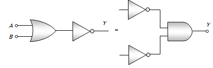
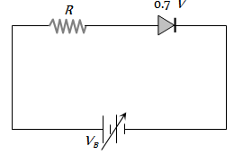
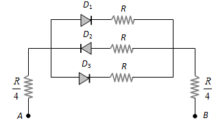
Questions · Page 3 of 9

M.C.Q (1 Marks)

MCQ 1011 Mark
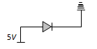
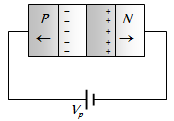
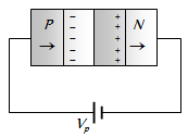
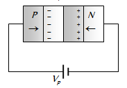
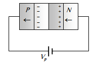
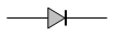
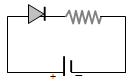
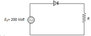
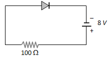
For the given circuit of $PN-$junction diode, which of the following statement is correct
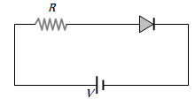
  • In forward biasing the voltage across $R$ is $V$
  • B
    In forward biasing the voltage across $R$ is $2V$
  • C
    In reverse biasing the voltage across $R$ is $V$
  • D
    In reverse biasing the voltage across $R$ is $2V$
Answer
Correct option: A.
In forward biasing the voltage across $R$ is $V$
View full question & answer
MCQ 1031 Mark
In the case of forward biasing of $PN-$junction, which one of the following figures correctly depicts the direction of flow of carriers
  • A
     
  • B
     
  •  
  • D
Answer
Correct option: C.
 
View full question & answer
Question 1051 Mark
P-type semiconductor is formed when
A. As impurity is mixed in Si                                                                         B. Al impurity is mixed in Si
C. B impurity is mixed in Ge                                                                         D. P impurity is mixed in Ge(a) A and C(b) A and D(c) B and C(d) B and D
       
Answer
(c) B and C
View full question & answer
MCQ 1061 Mark
Assertion   : The following circuit represents $'OR\ '$ gate

Reason : For the above circuit $Y=\bar{X}=\overline{\overline{A+B}}=A+B$
  • If both assertion and reason are true and the reason is the correct explanation of the assertion.
  • B
    If both assertion and reason are true but reason is not the correct explanation of the assertion.
  • C
    If assertion is true but reason is false.
  • D
    If the assertion and reason both are false.
Answer
Correct option: A.
If both assertion and reason are true and the reason is the correct explanation of the assertion.
View full question & answer
MCQ 1071 Mark
The symbol given in figure represents
  • $\text{NPN}$ transistor
  • B
    $\text{PNP}$ transistor
  • C
    Forward biased $\text{PN}$ junction diode
  • D
    Reverse biased $\text{NP}$ junction diode
Answer
Correct option: A.
$\text{NPN}$ transistor
View full question & answer
MCQ 1081 Mark
Assertion  : De$-$morgan's theorem $\overline{A+B}=\bar{A} \cdot \bar{B}$  may be explained by the following circuit

Reason  :  In the following circuit, for output inputs $\text{ABC}$ are $101$
  • A
    If both assertion and reason are true and the reason is the correct explanation of the assertion.
  • B
    If both assertion and reason are true but reason is not the correct explanation of the assertion.
  • If assertion is true but reason is false.
  • D
    If the assertion and reason both are false.
Answer
Correct option: C.
If assertion is true but reason is false.
View full question & answer
Question 1091 Mark
Assertion  :  NOT gate is also called inverter circuit.
Reason      : NOT gate inverts the input order.(a) If both assertion and reason are true and the reason is the correct explanation of the assertion.(b) If both assertion and reason are true but reason is not the correct explanation of the assertion.(c) If assertion is true but reason is false.(d) If the assertion and reason both are false.


Answer
(a) If both assertion and reason are true and the reason is the correct explanation of the assertion.
View full question & answer
Question 1101 Mark
Assertion  :  Zener diode works on a principle of breakdown voltage.
Reason      : Current increases suddenly after breakdown voltage.(a) If both assertion and reason are true and the reason is the correct explanation of the assertion.(b) If both assertion and reason are true but reason is not the correct explanation of the assertion.(c) If assertion is true but reason is false.(d) If the assertion and reason both are false.


Answer
(a) If both assertion and reason are true and the reason is the correct explanation of the assertion.
View full question & answer
Question 1111 Mark
Assertion : V-i characteristic of P-N junction diode is same as that of any other conductor.
Reason     : P-N junction diode behave as conductor at room temperature.(a) If both assertion and reason are true and the reason is the correct explanation of the assertion.(b) If both assertion and reason are true but reason is not the correct explanation of the assertion.(c) If assertion is true but reason is false.(d) If the assertion and reason both are false.


Answer
(d) If the assertion and reason both are false.
View full question & answer
Question 1121 Mark
Assertion :   At 0 K Germanium is a superconductor. 
Reason    :    At 0 K Germanium offers zero resistance.(a) If both assertion and reason are true and the reason is the correct explanation of the assertion.(b) If both assertion and reason are true but reason is not the correct explanation of the assertion.(c) If assertion is true but reason is false.(d) If the assertion and reason both are false.


Answer
(d) If the assertion and reason both are false.
View full question & answer
Question 1131 Mark
Assertion  :  NAND or NOR gates are called digital building blocks.
Reason      : The repeated use of NAND (or NOR) gates can produce all the basic or complicated gates.(a) If both assertion and reason are true and the reason is the correct explanation of the assertion.(b) If both assertion and reason are true but reason is not the correct explanation of the assertion.(c) If assertion is true but reason is false.(d) If the assertion and reason both are false.


Answer
(a) If both assertion and reason are true and the reason is the correct explanation of the assertion.
View full question & answer
Question 1141 Mark
Assertion :  A transistor is a voltage-operating device.
Reason     : Base current is greater than the collector current.(a) If both assertion and reason are true and the reason is the correct explanation of the assertion.(b) If both assertion and reason are true but reason is not the correct explanation of the assertion.(c) If assertion is true but reason is false.(d) If the assertion and reason both are false.


Answer
(d) If the assertion and reason both are false.
View full question & answer
Question 1151 Mark
Assertion  :  In transistor common emitter mode as an amplifier is preferred over common base mode.
Reason     : In common emitter mode the input signal is connected in series with the voltage applied to the base emitter function.(a) If both assertion and reason are true and the reason is the correct explanation of the assertion.(b) If both assertion and reason are true but reason is not the correct explanation of the assertion.(c) If assertion is true but reason is false.(d) If the assertion and reason both are false.


Answer
(b) If both assertion and reason are true but reason is not the correct explanation of the assertion.
View full question & answer
Question 1161 Mark
Assertion  :  Two P-N junction diodes placed back to back, will work as a NPN transistor.
Reason     : The P-region of two PN junction diodes back to back will form the base of NPN transistor.(a) If both assertion and reason are true and the reason is the correct explanation of the assertion.(b) If both assertion and reason are true but reason is not the correct explanation of the assertion.(c) If assertion is true but reason is false.(d) If the assertion and reason both are false.


Answer
(d) If the assertion and reason both are false.
View full question & answer
Question 1171 Mark
Assertion  :   Semiconductors do not Obey's Ohm's law. 
Reason     : Current is determined by the rate of flow of charge carriers.(a) If both assertion and reason are true and the reason is the correct explanation of the assertion.(b) If both assertion and reason are true but reason is not the correct explanation of the assertion.(c) If assertion is true but reason is false.(d) If assertion is false but reason is true.


Answer
(d) If assertion is false but reason is true.
View full question & answer
Question 1181 Mark
Assertion :   We can measure the potential barrier of a PN junction by putting a sensitive voltmeter across its terminals.
Reason     : The current through the PN junction is not same in forward and reversed bias.(a) If both assertion and reason are true and the reason is the correct explanation of the assertion.(b) If both assertion and reason are true but reason is not the correct explanation of the assertion.(c) If assertion is true but reason is false.(d) If assertion is false but reason is true.


Answer
(d) If assertion is false but reason is true.
View full question & answer
Question 1191 Mark
Assertion  :   Silicon is preferred over germanium for making semiconductor devices.
Reason      : The energy gap for germanium is more than the energy gap of silicon.(a) If both assertion and reason are true and the reason is the correct explanation of the assertion.(b) If both assertion and reason are true but reason is not the correct explanation of the assertion.(c) If assertion is true but reason is false.(d) If the assertion and reason both are false.


Answer
(c) If assertion is true but reason is false.
View full question & answer
Question 1201 Mark
Assertion  : If the temperature of a semiconductor is increased then it's resistance decreases.
Reason      : The energy gap between conduction band and valence band is very small(a) If both assertion and reason are true and the reason is the correct explanation of the assertion.(b) If both assertion and reason are true but reason is not the correct explanation of the assertion.(c) If assertion is true but reason is false.(d) If the assertion and reason both are false.


Answer
(a) If both assertion and reason are true and the reason is the correct explanation of the assertion.
View full question & answer
Question 1211 Mark
Assertion :   Base in a transistor is made very thin as compared to collector and emitter regions.                
Reason     : Due to thin base power gain and voltage gain is obtained by a transistor.(a) If both assertion and reason are true and the reason is the correct explanation of the assertion.(b) If both assertion and reason are true but reason is not the correct explanation of the assertion.(c) If assertion is true but reason is false.(d) If the assertion and reason both are false.


Answer
(a) If both assertion and reason are true and the reason is the correct explanation of the assertion.
View full question & answer
Question 1221 Mark
Assertion : The resistivity of a semiconductor increases with temperature.
Reason     : The atoms of a semiconductor vibrate with larger amplitude at higher temperature there by increasing it's resistivity.(a) If both assertion and reason are true and the reason is the correct explanation of the assertion.(b) If both assertion and reason are true but reason is not the correct explanation of the assertion.(c) If assertion is true but reason is false.(d) If the assertion and reason both are false.


Answer
(d) If the assertion and reason both are false.
View full question & answer
Question 1231 Mark
Assertion  :  A transistor amplifier in common emitter configuration has a low input impedence.
Reason      : The base to emitter region is forward biased.(a) If both assertion and reason are true and the reason is the correct explanation of the assertion.(b) If both assertion and reason are true but reason is not the correct explanation of the assertion.(c) If assertion is true but reason is false.(d) If the assertion and reason both are false.


Answer
(a) If both assertion and reason are true and the reason is the correct explanation of the assertion.
View full question & answer
Question 1241 Mark
Assertion : In a common emitter transistor amplifier the input current is much less than the output current.
Reason     : The common emitter transistor amplifier has very high input impedance.(a) If both assertion and reason are true and the reason is the correct explanation of the assertion.(b) If both assertion and reason are true but reason is not the correct explanation of the assertion.(c) If assertion is true but reason is false.(d) If the assertion and reason both are false.


Answer
(c) If assertion is true but reason is false.
View full question & answer
MCQ 1251 Mark
The given figure shows the wave forms for two inputs $A$ and $B$ and that for the output $Y$ of a logic circuit. The logic circuit is
  • An $\text{AND}$ gate
  • B
    An $\text{OR}$ gate
  • C
    A $\text{NAND}$ gate
  • D
    An $\text{NOT}$ gate
Answer
Correct option: A.
An $\text{AND}$ gate
View full question & answer
MCQ 1261 Mark
The slopes of anode and mutual characteristics of a triode are $0.02\ mA\  V^{–1}$ and $1\ mA\  V^{–1}$ respectively. What is the amplification factor of the valve
  • A
    $5$
  • $50$
  • C
    $500$
  • D
    $0.5$
Answer
Correct option: B.
$50$
$50$
View full question & answer
Question 1271 Mark
Amplification factor of a triode is 10. When the plate potential is 200 volt and grid potential is – 4 volt, then the plate current of 4mA is observed. If plate potential is changed to 160 volt and grid potential is kept at – 7 volt, then the plate current will be(a) 1.69 mA(b) 3.95 mA(c) 2.87 mA(d) 7.02 mA
       
Answer
(a) 1.69 mA
View full question & answer
MCQ 1281 Mark
For a triode $m = 64$ and $g_m =1600m$ mho. It is used as an amplifier and an input signal of $1V\ (rms)$ is applied. The signal power in the load of $40\ kW$ will be
  • A
    $23.5\ mW$
  • B
    $48.7\ mW$
  • $25.6\ mW$
  • D
    None of these
Answer
Correct option: C.
$25.6\ mW$
$25.6\ mW$
View full question & answer
Question 1291 Mark
A triode whose mutual conductance is 2.5 m A/volt and anode resistance is 20 kilo ohm, is used as an amplifier whose amplification is 10. The resistance connected in plate circuit will be(a) 1 kW  (b) 5 kW(c) 10 kW(d) 20 kW
       
Answer
(b) 5 kW
View full question & answer
Question 1301 Mark
A change of 0.8 mA in the anode current of a triode occurs when the anode potential is changed by 10 V. If m = 8 for the triode, then what change in the grid voltage would be required to produce a change of 4 mA in the anode current(a) 6.25 V(b) 0.16 V(c) 15.2 V(d) None of these
       
Answer
(a) 6.25 V
View full question & answer
Question 1311 Mark
A metallic surface with work function of 2 eV, on heating to a temperature of 800 K gives an emission current of 1 mA. If another metallic surface having the same surface area, same emission constant but work function 4 eV is heated to a temperature of 1600 K, then the emission current will be(a) 1 mA(b) 2 mA(c) 4 mA(d) None of these
       
Answer
(c) 4 mA
View full question & answer
MCQ 1321 Mark
The junction diode in the following circuit requires a minimum current of $1\ mA$ to be above the knee point $(0.7 V)$ of its $I-V$ characteristic curve. The voltage across the diode is independent of current above the knee point. If $V_B = 5V,$ then the maximum value of $R$ so that the voltage is above the knee point, will be
  • $4.3\ kW $
  • B
    $860\ kW$
  • C
    $4.3\ W $
  • D
    $860\ W$
Answer
Correct option: A.
$4.3\ kW $
$4.3\ kW $
View full question & answer
MCQ 1331 Mark
A sinusoidal voltage of peak value $200$ volt is connected to a diode and resistor $R$ in the circuit shown so that half wave rectification occurs. If the forward resistance of the diode is negligible compared to $R$ the rms voltage $($in volt$)$ across $R$ is approximately
  • A
    $200$
  • $100$
  • C
    $\frac{200}{\sqrt{2}}$ 
  • D
    $280$
Answer
Correct option: B.
$100$
$100$
View full question & answer
MCQ 1341 Mark
In a negative logic the following wave form corresponds to the
  • A
    $0000000000$
  • B
    $0101101000$
  • C
    $1111111111$
  • $1010010111$
Answer
Correct option: D.
$1010010111$
$1010010111$
View full question & answer
MCQ 1351 Mark
The diode used in the circuit shown in the figure has a constant voltage drop of $0.5 V$ at all currents and a maximum power rating of $100$ milliwatts. What should be the value of the resistor $R,$ connected in series with the diode for obtaining maximum current
  • A
    $1.5 W$
  • $5 W$
  • C
    $6.67 W$
  • D
    $200 W$
Answer
Correct option: B.
$5 W$
$5 W$
View full question & answer
MCQ 1361 Mark
The $i-V$ characteristic of a $P-N$ junction diode is shown below. The approximate dynamic resistance of the $P-N$ junction when a forward bias of $2$ volt is applied
  • A
    $1 \Omega$
  • $0.25 \Omega$
  • C
    $0.5 \Omega$
  • D
    $5 \Omega$
Answer
Correct option: B.
$0.25 \Omega$
$0.25 \Omega$
View full question & answer
MCQ 1371 Mark
A source voltage of $8V$ drives the diode in fig. through a current$-$limiting resistor of $100$ ohm. Then the magnitude of the slope load line on the $V-I$ characteristics of the diode is
  • $0.01$
  • B
    $100$
  • C
    $0.08$
  • D
    $12.5$
Answer
Correct option: A.
$0.01$
$0.01$
View full question & answer
MCQ 1381 Mark
The  relation between dynamic plate resistance $(r_{p­})$ of a vacuum diode and plate current in the space charge limited region, is
  • A
    $r_p \propto I_{p}$
  • B
    $r_p \propto I_p^{3 / 2}$
  • C
    $r_p \propto \frac{1}{I_p}$
  • $r_p \propto \frac{1}{\left(I_p\right)^{1 / s}}$
Answer
Correct option: D.
$r_p \propto \frac{1}{\left(I_p\right)^{1 / s}}$
View full question & answer
MCQ 1391 Mark
In $\text{NPN}$ transistor$, 10^{10}$ electrons enters in emitter region in $10^{–6} \sec$. If $2\%$ electrons are lost in base region then collector current and current amplification factor $(b)$ respectively are
  • $1.57\  mA, 49$
  • B
    $1.92 \ mA, 70$
  • C
    $2\ mA, 25$
  • D
    $2.25\ mA, 100$
Answer
Correct option: A.
$1.57\  mA, 49$
$1.57\  mA, 49$
View full question & answer
MCQ 1401 Mark
The combination of gates shown below produces
  • A
    $\text{AND}$ gate
  • B
    $\text{XOR}$ gate
  • C
    $\text{NOR}$ gate
  • $\text{NAND}$ gate 
Answer
Correct option: D.
$\text{NAND}$ gate 
$\text{NAND}$ gate 
View full question & answer
MCQ 1411 Mark
For the transistor circuit shown below, if $b = 100,$ voltage drop between emitter and base is $0.7 V$ then value of $V_{CE}$ will be
  • A
    $10 V$
  • $5 V$
  • C
    $13 V $
  • D
    $0 V$
Answer
Correct option: B.
$5 V$
$13 V $
View full question & answer
MCQ 1421 Mark
The contribution in the total current flowing through a semiconductor due to electrons and holes are $\frac{3}{4}$  and $\frac{1}{4}$  respectively. If the drift velocity of electrons is $\frac{5}{2}$  times that of holes at this temperature, then the ratio of concentration of electrons and holes is
  • $6 : 5$
  • B
    $5 : 6$
  • C
    $3 : 2$
  • D
    $2 : 3$
Answer
Correct option: A.
$6 : 5$
$6 : 5$
View full question & answer
MCQ 1431 Mark
A potential difference of $2 V$ is applied between the opposite faces of a $Ge$ crystal plate of area $1\ cm^2$ and thickness $0.5\  mm$ . If the concentration of electrons in $Ge$ is $2 \times 10^{19} / m ^3$ and mobilities of electrons and holes are $0.36 \frac{m^2}{ volt - sec }$ and $0.14 \frac{m^2}{ volt - sec }$ respectively, then the current flowing through the plate will be
  • A
    $0.25 A$
  • B
    $0.45 A$
  • C
    $0.56 A$
  • $0.64 A$
Answer
Correct option: D.
$0.64 A$
$0.64 A$
View full question & answer
MCQ 1441 Mark
The plate current $i_p$ in a triode valve is given $i_p=K\left(V_p+\mu V_g\right)^{3 / 2}$ where $i_p$ is in milliampere and $V_p$ and $V_g$ are in volt. If $r_p=10^4$ ohm, and $g_m=5 \times 10^{-3} \ mho$, then for ${ }^{i_p}=8 mA$ and $V_p=300$ volt, what is the value of K and grid cut off voltage
  • A
    $-6 V , (30)^{3 / 2}$
  • $-6 V,(1 / 30)^{3 / 2}$
  • C
    $+6 V,(30)^{3 / 2}$
  • D
    $+6 V,(1 / 30)^{3 / 2}$
Answer
Correct option: B.
$-6 V,(1 / 30)^{3 / 2}$
View full question & answer
MCQ 1461 Mark
In the following circuits $PN-$junction diodes $D_1, D_2$ and $D_3$ are ideal for the following potential of $A$ and $B,$ the correct increasing order of resistance between $A$ and $B$ will be

$\ce{(i) – 10 V, – 5V (ii)  – 5V, – 10 V   (iii) – 4V, – 12V}$
  • A
    $(i) < (ii) < (iii)$
  • $(iii) < (ii) < (i)$
  • C
    $(ii) = (iii) < (i)$
  • D
    $ (i) = (iii) < (ii)$
Answer
Correct option: B.
$(iii) < (ii) < (i)$
View full question & answer
Question 1471 Mark
The Bohr radius of the fifth electron of phosphorus (atomic number = 15) acting as dopant in silicon (relative dielectric constant = 12) is(a) 10.6 Å(b) 0.53 Å(c) 21.2 Å                                           (d) None of these
       
Answer
(a) 10.6 Å
View full question & answer
MCQ 1481 Mark
The circuit shown in following figure contains two diode $D_1$ and $D_2$ each with a forward resistance of $50$ ohms and with infinite backward resistance. If the battery voltage is $6 V,$ the current through the $100$ ohm resistance $($in amperes$)$ is
  • A
    Zero
  • $0.02$
  • C
    $0.03$
  • D
    $0.036$
Answer
Correct option: B.
$0.02$
$0.02$
View full question & answer
Question 1491 Mark
A transistor is used as an amplifier in CB mode with a load resistance of 5 k W the current gain of amplifier is 0.98 and the input resistance is 70 W, the voltage gain and power gain respectively are(a) 70, 68.6(b) 80, 75.6(c) 60, 66.6(d) 90, 96.6
       
Answer
(a) 70, 68.6
View full question & answer
MCQ 1501 Mark
The peak voltage in the output of a half$-$wave diode rectifier fed with a sinusoidal signal without filter is $10 V.$ The dc component of the output voltage is
  • A
    $10 /{\sqrt{2} V}$
  • $10 / \mathrm{p} \mathrm{V}$
  • C
    $10\ V$
  • D
    $20 / \mathrm{p} \mathrm{V}$
Answer
Correct option: B.
$10 / \mathrm{p} \mathrm{V}$
View full question & answer