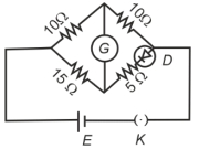
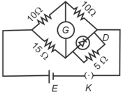
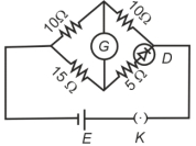
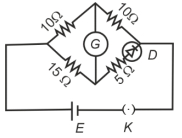
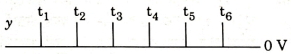
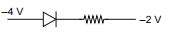
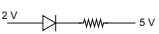
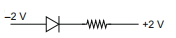
MCQ 11 Mark
Choose the correct circuit which can achieve the bridge balance.
Answerd
In option ($4$),
$\frac{10}{15}=\frac{10}{5+R_D}$
The diode can conduct and have resistance $R_D=10 \Omega$ because diode have dynamic resistance. In that case bridge will be balanced.
View full question & answer→MCQ 21 Mark
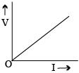
Consider the following statements $\mathrm{A}$ and $\mathrm{B}$ and identify the correct answer:
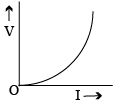
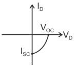
$A$. For a solar-cell, the $I-V$ characteristics lies in the $IV$ quadrant of the given graph.
$B$. In a reverse biased $p n$ junction diode, the current measured in $(\mu \mathrm{A})$, is due to majority charge carriers.
- A
$A$ is incorrect but $B$ is correct
- B
Both $A$ and $B$ are correct
- C
Both $A$ and $B$ are incorrect
- ✓
$A$ is correct but $B$ is incorrect
AnswerCorrect option: D. $A$ is correct but $B$ is incorrect
d
Solar cell characteristics
(image)
$B$: In reverse biased $p n$ junction diode, the current measured in $(\mu A)$, is due to minority charge carrier.
View full question & answer→MCQ 31 Mark
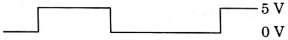
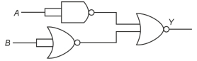
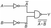
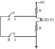
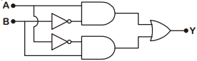
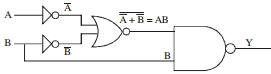
The output ( $Y$ ) of the given logic gate is similar to the output of an/a
- A
$NOR$ gate
- B
$OR$ gate
- ✓
$AND$ gate
- D
$NAND$ gate
AnswerCorrect option: C. $AND$ gate
c
$Y_1 =\overline{A \cdot A}$
$=\bar{A}$
$Y_2 =\overline{B+B}$
$=\bar{B}$
$Y =\overline{Y_1+Y_2}$
$=\overline{\bar{A}+\bar{B}}$
$=\overline{\bar{A}} \cdot \overline{\bar{B}}$
$=A \cdot B$ is similar to output of $AND$ Gate
View full question & answer→MCQ 41 Mark
A logic circuit provides the output $Y$ as per the following truth table :
| $A$ |
$B$ |
$Y$ |
| $0$ |
$0$ |
$1$ |
| $0$ |
$1$ |
$0$ |
| $1$ |
$0$ |
$1$ |
| $1$ |
$1$ |
$0$ |
The expression for the output $Y$ is :
AnswerCorrect option: B. $\bar{B}$
b
| $A$ |
$B$ |
$Y$ |
| $0$ |
$0$ |
$1$ |
| $0$ |
$1$ |
$0$ |
| $1$ |
$0$ |
$1$ |
| $1$ |
$1$ |
$0$ |
According to given truth table, output is independent on value of $A$
$\therefore$ Output $Y=\bar{B}$
View full question & answer→MCQ 51 Mark
Given below are two statements:
Statement $I$ : Photovoltaic devices can convert optical radiation into electricity.
Statement $II$ : Zener diode is designed to operate under reverse bias in breakdown region.
In the light of the above statements, choose the most appropriate answer from the options given below
- A
Statement $I$ is incorrect but Statement $II$ is correct.
- ✓
Both Statement $I$ and Statement $II$ are correct
- C
Both Statement $I$ and Statement $II$ are incorrect.
- D
Statement $I$ is correct but Statement $II$ is incorrect.
AnswerCorrect option: B. Both Statement $I$ and Statement $II$ are correct
b
Statement $I$ : Photocell/solar cell convert light energy into electric energy/current.
Statement $II$ : We use zener diode in reverse biased condition, when reverse biased voltage more than break down voltage than it act as stablizer.
View full question & answer→MCQ 61 Mark
For the following logic circuit, the truth table is:
- A
| $A$ |
$B$ |
$Y$ |
| $0$ |
$0$ |
$0$ |
| $0$ |
$1$ |
$0$ |
| $1$ |
$0$ |
$0$ |
| $1$ |
$1$ |
$1$ |
- B
| $A$ |
$B$ |
$Y$ |
| $0$ |
$0$ |
$1$ |
| $0$ |
$1$ |
$1$ |
| $1$ |
$0$ |
$1$ |
| $1$ |
$1$ |
$0$ |
- ✓
| $A$ |
$B$ |
$Y$ |
| $0$ |
$0$ |
$0$ |
| $0$ |
$1$ |
$1$ |
| $1$ |
$0$ |
$1$ |
| $1$ |
$1$ |
$1$ |
- D
| $A$ |
$B$ |
$Y$ |
| $0$ |
$0$ |
$1$ |
| $0$ |
$1$ |
$0$ |
| $1$ |
$0$ |
$1$ |
| $1$ |
$1$ |
$0$ |
AnswerCorrect option: C.
| $A$ |
$B$ |
$Y$ |
| $0$ |
$0$ |
$0$ |
| $0$ |
$1$ |
$1$ |
| $1$ |
$0$ |
$1$ |
| $1$ |
$1$ |
$1$ |
c
$Y=\overline{\bar{A} \cdot \bar{B}}=A+B$
It is $OR$ gate.
| $A$ |
$B$ |
$Y$ |
| $0$ |
$0$ |
$0$ |
| $0$ |
$1$ |
$1$ |
| $1$ |
$0$ |
$1$ |
| $1$ |
$1$ |
$1$ |
View full question & answer→MCQ 71 Mark
A full wave rectifier circuit consists of two $p-n$ junction diodes, a centre-tapped transformer, capacitor and a load resistance. Which of these components remove the ac ripple from the rectified output?
- A
- B
A centre-tapped transformer
- C
- ✓
Answerd
Capacitor used to remove $AC$ ripples from Rectifier output.
View full question & answer→MCQ 81 Mark
In the given circuits $(a)$,$(b)$ and $(c)$, the potential drop across the two p-n junctions are equal in:
AnswerCorrect option: C. Both circuits $(a)$ and $(c)$
c
In $(a)$ $\&$ $(c)$ circuits, both the junctions are in same biasing conditions so offers equal resistances.
Since both are in series, therefore equal potential will drop across the junction.
View full question & answer→MCQ 91 Mark
The incorrect statement about the property of a Zener diode is
AnswerCorrect option: C. Depletion region formed is very wide
c
For zener diode $\rightarrow$ Doping is high
Depletion region is thin
It is operated in Reverse Bias region
Zener voltage $\left( V _{ z }\right)$ is constant
View full question & answer→MCQ 101 Mark
The collector current in a common base amplifier using $n-p-n$ transistor is $24\; mA$. If $80 \%$ of the electrons released by the emitter is accepted by the collector, then the base current is numerically
- A
$6\,mA$ and leaving the base
- B
$3\,mA$ and leaving the base
- ✓
$6\,mA$ and entering the base
- D
$3\,mA$ and entering the base
AnswerCorrect option: C. $6\,mA$ and entering the base
c
$I _C=24\,mA$
$\text { and } I _{ E }=\frac{ I _{ C }}{\alpha}$
$I _{ E }=\frac{24 mA }{0.8}=30\,mA$
$\therefore I _{ B }= I _{ E }- I _C$
$=6\,mA \text { (into the base) }$
View full question & answer→MCQ 111 Mark
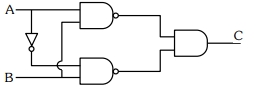
The Truth table for the given logic circuit is:
- A
| $A$ |
$B$ |
$C$ |
| $0$ |
$1$ |
$0$ |
| $0$ |
$1$ |
$0$ |
| $1$ |
$0$ |
$0$ |
| $1$ |
$1$ |
$1$ |
- ✓
| $A$ |
$B$ |
$C$ |
| $0$ |
$0$ |
$1$ |
| $0$ |
$1$ |
$0$ |
| $1$ |
$0$ |
$1$ |
| $1$ |
$1$ |
$0$ |
- C
| $A$ |
$B$ |
$C$ |
| $0$ |
$0$ |
$0$ |
| $0$ |
$1$ |
$0$ |
| $1$ |
$0$ |
$0$ |
| $1$ |
$1$ |
$1$ |
- D
| $A$ |
$B$ |
$C$ |
| $0$ |
$0$ |
$0$ |
| $0$ |
$1$ |
$1$ |
| $1$ |
$0$ |
$1$ |
| $1$ |
$1$ |
$0$ |
AnswerCorrect option: B.
| $A$ |
$B$ |
$C$ |
| $0$ |
$0$ |
$1$ |
| $0$ |
$1$ |
$0$ |
| $1$ |
$0$ |
$1$ |
| $1$ |
$1$ |
$0$ |
b
$C=\overline{A \cdot B} \cdot \bar{A} \cdot B$
using De-Morgan Theorem
$C=\overline{A \cdot B+\bar{A} \cdot B}$
$C=\overline{B(A+\bar{A})}=\bar{B}$
Therefore
| $A$ |
$B$ |
$C$ |
| $0$ |
$0$ |
$1$ |
| $0$ |
$1$ |
$0$ |
| $1$ |
$0$ |
$1$ |
| $1$ |
$1$ |
$0$ |
View full question & answer→MCQ 121 Mark
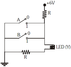
Identify the equivalent logic gate represented by the given circuit
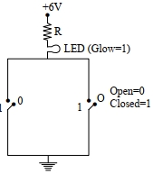
Answera
Here, current flows when any of the switch is in $ON$ $(1)$ state.
| $A$ |
$B$ |
$LED$ |
| $0$ |
$0$ |
$0$ |
| $0$ |
$1$ |
$1$ |
| $1$ |
$0$ |
$1$ |
| $1$ |
$1$ |
$1$ |
$OR$ Gate
View full question & answer→MCQ 131 Mark
As the temperature increases, the electrical resistance
- A
decreases for both conductors and semiconductors
- ✓
increases for conductors but decreases for semiconductors
- C
decreases for conductors but increases for semiconductors
- D
increases for both conductors and semiconductors
AnswerCorrect option: B. increases for conductors but decreases for semiconductors
b
For conductors $\alpha$ is $(+)ve$
For semiconductors and Insulators $\alpha$ is $(-)ve$
View full question & answer→MCQ 141 Mark
In half wave rectification, if the input frequency is $60\,Hz$, then the output frequency would be$\dots\dots\dots\,Hz$
Answerb
In half wave rectification
$f_{\text {in }}=f_{\text {out }}$
$\Rightarrow f_{\text {out }}=60 Hz$
View full question & answer→MCQ 151 Mark
The electron concentration in an $n-$type semiconductor is the same as hole concentration in a $p-$type semiconductor. An external field (electric) is applied across each of them. Compare the currents in them.
- A
current in $\mathrm{n}$-type $=$ current in $\mathrm{p}$-type.
- B
current in $p-$type $>$ current in $\mathrm{n}$-type.
- ✓
current in $\mathrm{n}$-type $>$ current in $\mathrm{p}$-type.
- D
No current will flow in $p$-type, current will only flow in $\mathrm{n}$-type.
AnswerCorrect option: C. current in $\mathrm{n}$-type $>$ current in $\mathrm{p}$-type.
c
In $N$ type semiconductor majority charge carriersare $\mathrm{e}^{-}$and $\mathrm{P}$ type semiconductor majority chargecarriers are holes.
$I=\operatorname{neAV}_{d}=\operatorname{neA}(\mu \mathrm{E})$
$\mu_{\mathrm{e}}>\mu_{\mathrm{h}}=\mathrm{I}_{\mathrm{e}}>\mathrm{I}_{\mathrm{h}}$
View full question & answer→MCQ 161 Mark
Consider the following statements $(A)$ and $(B)$ and identify the correct answer.
$(A)$ A zener diode is connected in reverse bias, when used as a voltage regulator.
$(B)$ The potential barrier of $\mathrm{p}-\mathrm{n}$ junction lies between $0.1\, \mathrm{~V}$ to $0.3 \,\mathrm{~V}$.
- A
$(A)$ and $(B)$ both are correct.
- B
$(A)$ and $(B)$ both are incorrect.
- ✓
$(A)$ is correct and $(B)$ is incorrect.
- D
$(A)$ is incorrect but $(B)$ is correct.
AnswerCorrect option: C. $(A)$ is correct and $(B)$ is incorrect.
c
Reverse bias Zener diode use as a voltage regulator
for Ge Potential barrier $\mathrm{V}_{0}=0.3\, \mathrm{~V}$
Si Potential barrier $\mathrm{V}_{0}=0.7\, \mathrm{~V}$
View full question & answer→MCQ 171 Mark
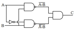
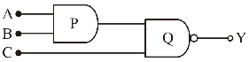
For the given circuit, the input digital signals are applied at the terminals $\mathrm{A}, \mathrm{B}$ and $\mathrm{C}$. What would be the output at the terminal $y$ ?
Answerc
$\frac{\mathrm{AB}}{\mathrm{BC}}$
$\mathrm{Y}=\mathrm{AB}+\overline{\mathrm{BC}}$
| $A$ |
$B$ |
$C$ |
$Y$ |
| $0$ |
$0$ |
$1$ |
$0+1=1$ |
| $1$ |
$0$ |
$1$ |
$0+1=1$ |
| $0$ |
$1$ |
$0$ |
$0+1=1$ |
| $0$ |
$0$ |
$1$ |
$0+1=1$ |
View full question & answer→MCQ 181 Mark
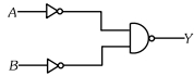
For the logic circuit shown, the truth table is :
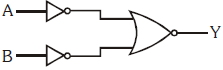
- A
$\begin{array}{lll}\text {A} & \text {B} & \text {Y} \\ 0 & 0 & 1 \\ 0 & 1 & 0 \\ 1 & 0 & 0 \\ 1 & 1 & 0\end{array}$
- ✓
$\begin{array}{lll}\text {A} & \text {B} & \text {Y} \\ 0 & 0 & 0 \\ 0 & 1 & 0 \\ 1 & 0 & 0 \\ 1 & 1 & 1\end{array}$
- C
$\begin{array}{lll}\text {A} & \text {B} & \text {Y} \\ 0 & 0 & 0 \\ 0 & 1 & 1 \\ 1 & 0 & 1 \\ 1 & 1 & 1\end{array}$
- D
$\begin{array}{lll}\text {A} & \text {B} & \text {Y} \\ 0 & 0 & 1 \\ 0 & 1 & 1 \\ 1 & 0 & 1 \\ 1 & 1 & 0\end{array}$
AnswerCorrect option: B. $\begin{array}{lll}\text {A} & \text {B} & \text {Y} \\ 0 & 0 & 0 \\ 0 & 1 & 0 \\ 1 & 0 & 0 \\ 1 & 1 & 1\end{array}$
b
$Y=\overline{\bar{A}+\bar{B}}=\overline{\bar{A}} \cdot \overline{\bar{B}}=A \cdot B=$ $AND$ gate
$\begin{array}{lll}\text {A} & \text {B} & \text {Y} \\ 0 & 0 & 0 \\ 0 & 1 & 0 \\ 1 & 0 & 0 \\ 1 & 1 & 1\end{array}$
View full question & answer→MCQ 191 Mark
Which of the following gate is called universal gate ?
- A
$NOT$ gate
- B
$OR$ gate
- C
$AND$ gate
- ✓
$NAND$ gate
AnswerCorrect option: D. $NAND$ gate
d
With the help of $NAND$ gate any logic function or gate can be realized. Hence it is called as universal gate.
View full question & answer→MCQ 201 Mark
The solids which have the negative temperature coefficient of resistance are :
- ✓
Insulators and semiconductors
- B
- C
- D
AnswerCorrect option: A. Insulators and semiconductors
a
The negative temperature coefficient of the resistance is only present in the insulators or the semiconductors. In these, the resistance decreases with increase in temperature.
View full question & answer→MCQ 211 Mark
An intrinsic semiconductor is converted into $N$-type extrinsic semiconductor by doping it with
Answerb
When intrinsic semiconductor (Si or Ge) is doped with a pentavalent element, e.g. $\begin{array}{ll}\text { phosphorus }( P ), & \text { a n-type extrinsic }\end{array}$ semiconductor is created because
pentavalent dopant donates one extra electron for conduction.
View full question & answer→MCQ 221 Mark
The increase in the width of depletion reglon in a $p-n$ junction diode is due to
- A
increase in forward current
- B
- ✓
- D
both forward bias and reverse bias
Answerc
In reverse bias external battery attract majority charge carriers.
so width of the depletion region increase
View full question & answer→MCQ 231 Mark
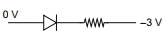
Out of the following which one is a forward biased diode?
Answera
In option (1), P-side is connected to the higher potential $\left(V_{H}=0 V\right)$ and $N-$ side is connected to the lower potential $\left(V_{L}=-3 \vee\right) .$ Hence, it is forward biased.
View full question & answer→MCQ 241 Mark
For transistor action, which of the following statements is correct$?$
- ✓
The base region must be very thin and lightly doped.
- B
Base, emitter and collector regions should have same doping concentrations.
- C
Base, emitter and collector regions should have same size.
- D
Both emitter junction as well as the collector Junction are forward biased.
AnswerCorrect option: A. The base region must be very thin and lightly doped.
a
Base region is very thin and lightly doped.
View full question & answer→MCQ 251 Mark
A $N-P-N$ transistor is connected in common emitter configuration (see figure) in which collector voltage drop across load resistance $(800 \; \Omega)$ connected to the collector circuit is $0.8 \;V$. The collector current is .............. $mA$
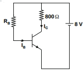
Answerd
Voltage drop across load resistance,
$V _{ L }= I _{ C } R _{ C }$
$0.8= I _{ C } \times 800$
$I _{ C }=1 mA$
View full question & answer→MCQ 261 Mark
For a $p-$type semiconductor which of the following statements is true ?
- A
Electrons are the majority carriers and trivalent atoms are the dopants.
- ✓
Holes are the majority carriers and trivalent atoms are the dopants.
- C
Holes are the majority carriers and pentavalent atoms are the dopants.
- D
Electrons are the majority carriers and pentavalent atoms are the dopants.
AnswerCorrect option: B. Holes are the majority carriers and trivalent atoms are the dopants.
b
For $P$ type Holes are majority and trivalent atoms are the dopants.
View full question & answer→MCQ 271 Mark
The correct Boolean operation represented by the circuit diagram drawn is
AnswerCorrect option: C. $NAND$
c
$\begin{array}{|c|c|c|}\hline A & {B} & {Y} \\ \hline 0 & {0} & {1} \\ \hline 0 & {1} & {1} \\ \hline 1 & {0} & {1} \\ \hline 1 & {1} & {0} \\ \hline\end{array}$
It is a $NAND$ Gate
View full question & answer→MCQ 281 Mark
The circuit diagram shown here corresponds to the logic gate,
Answera
$\begin{array}{|l|l|l|}\hline A & {B} & {Y} \\ \hline 0 & {0} & {1} \\ {0} & {1} & {0} \\ {1} & {0} & {0} \\ {1} & {1} & {0} \\ \hline\end{array}$
View full question & answer→MCQ 291 Mark
An $LED$ is constructed from a $p-n$ junction diode using $GaAsP$. The energy gap is $1.9\; eV$. The wavelength of the light emitted will be equal to
AnswerCorrect option: B. $654 \;nm$
b
$\lambda=\frac{1240 \mathrm{nm}}{1.9}=652.6 \mathrm{nm} \simeq 654\; \mathrm{nm}$
View full question & answer→MCQ 301 Mark
In a $p-n$ junction diode, change in temperature due to heating
AnswerCorrect option: C. affects the overall $V - I$ characteristics of $p-n$ junction
c
Due to heating, number of electron-hole pairs will increase, so overall resistance of diode will change.
Due to which forward biasing and reversed biasing both are changed.
View full question & answer→MCQ 311 Mark
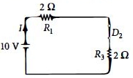
In the circuit shown in the figure, the input voltage $V_i$ is $20\,\, V, \,\,V_{BE} = 0 $ and $V_{CE}= 0.$ The values of $I_B\,,\,I_c$ and $\beta$ are given by
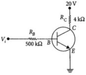
- A
$I_B=40$$\mu A$, $I_C=10mA$,$\;\;\beta $$=250$
- B
$I_B=25$$\mu A$, $I_C= 5 mA,$$\;\;\beta $$=200$
- ✓
$I_B=40$$\mu A$, $I_C = 5mA$,$\;\;\beta $$= 125$
- D
$I_B=20$$\mu A$,$ I_C = 5mA$,$\;\;\beta $$=250$
AnswerCorrect option: C. $I_B=40$$\mu A$, $I_C = 5mA$,$\;\;\beta $$= 125$
c
Given $V_{B E}=0$ ; $V_{C E}=0$
$\therefore \quad$ Collector current, $I_{C}=\frac{(20-0)}{4 \times 10^{3}}$
or $I_{C}=5 \times 10^{-3} \mathrm{A}=5\, \mathrm{mA}$
Input voltage, $V_{i}=V_{B E}+I_{B} R_{B}$
or $\quad V_{i}=0+I_{B} R_{B}$ or $20=I_{B} \times 500 \times 10^{3}$
$\therefore \quad I_{B}=\frac{20}{500 \times 10^{3}}=40\, \mu \mathrm{A}$
$\therefore $ Current gain, $\beta=\frac{I_{C}}{I_{B}}=\frac{5 \times 10^{-3}}{40 \times 10^{-6}}=125$
View full question & answer→MCQ 321 Mark
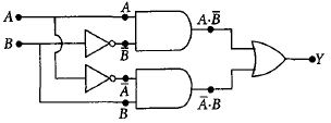
In the combination of the following gates the output $Y$ can be written in terms of inputs $A$ and $B$ as
AnswerCorrect option: B. $A\cdot \overline {B} + \overline {A} \cdot B$
b
View full question & answer→MCQ 331 Mark
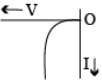
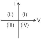
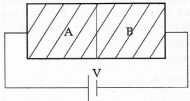
Two sides of a semiconductor germanium crystal $A$ and $B$ are doped with arsenic and indium respectively. They are connected to a battery as shown in figure. The correct graph between current and voltage for the arrangement is
View full question & answer→MCQ 341 Mark
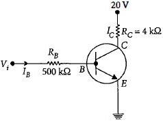
In a common emitter transistor amplifier the audio signal voltage across the collector is $3\,\, V.$ The resistance of collector is $3\,k\Omega $. If current gain is $100$ and the base resistance is $2\,k\Omega$, the voltage and power gain of the amplifier
- A
$15$ and $200$
- ✓
$150$ and $15000$
- C
$20$ and $2000$
- D
$200$ and $1000$
AnswerCorrect option: B. $150$ and $15000$
b
${{V}_{i}}=3\text{V},{{R}_{C}}=3\text{k}\Omega ,{{R}_{B}}=2\text{k}\Omega $
${\beta=100}$
Voltage gain of the $CE$ amplifier,
$A_{V}=-\beta_{a c}\left(\frac{R_{C}}{R_{B}}\right)=-100\left(\frac{3}{2}\right)=-150$
Power gain, $A_{P}=\beta \times A_{V}=100 \times(-150)$
$=-15000$
Negative sign represents that output voltage is in opposite phase with the input voltage.
View full question & answer→MCQ 351 Mark
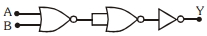
From the circuit of the following Logic gates, the basic logic gate obtained is
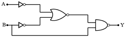
- A
$AND $ ગેટ
- B
$OR$ ગેટ
- C
$NOT $ ગેટ
- ✓
$NAND$ ગેટ
AnswerCorrect option: D. $NAND$ ગેટ
d
$Y =\overline{ AB \cdot B }=\overline{ AB }+\overline{ B }$
$=\overline{ A }+\overline{ B }+\overline{ B }$
$=\overline{ A }+\overline{ B }$
$Y =\overline{ A . B }$
$NAND$ Gate
View full question & answer→MCQ 361 Mark
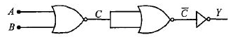
The given electrical network is equivalent to
- A
$AND$ gate
- B
$OR $ gate
- C
$NOT$ gate
- ✓
$NOR $ gate
AnswerCorrect option: D. $NOR $ gate
d
$\begin{array}{|l|l|l|l|l|}\hline A & {B} & {C} & {\bar{C}} & {\text { Output }(Y)} \\ \hline 0 & {0} & {1} & {0} & {1} \\ {0} & {1} & {0} & {1} & {0} \\ {1} & {0} & {0} & {1} & {0} \\ {1} & {1} & {0} & {1} & {0} \\ \hline\end{array}$
At output, the truth table corresponds to $NOR$ gate
View full question & answer→MCQ 371 Mark
A common emitter amplifier circuit is shown in the figure below. For the transistor used in the circuit the current amplification factor, ${\beta _{dc}} = 100$. Other parameters are mentioned in the figure.
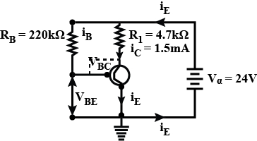
- A
$V_{BE}= +18.5 V , V_{BC}= +2.85$ and amplifier is not working.
- ✓
$V_{BE}= +20.7 V , V_{BC}= +3.75$ and amplifier is not working.
- C
$V_{BE}= +21.5 V , V_{BC}= -2.75$ and amplifier is working.
- D
$V_{BE}= +18.2 V , V_{BC}= -3.45 $ and amplifier is working.
AnswerCorrect option: B. $V_{BE}= +20.7 V , V_{BC}= +3.75$ and amplifier is not working.
b
$\beta=100$
$I _{ B }=\frac{ I _{ C }}{\beta}$
$I _{ B }=15 \mu A$
$V _{ CC }= I _{ B } R _{ B }+ V _{ BE }$
$V _{ BE }=24-\left(15 \times 10^{-6} \times 220 \times 10^{3}\right)$
$V _{ BE }=20.7 V$
$V _{ BC }= I _{ C } R _{ L }- I _{ B } R _{ B }=7.05-3.3=3.75 V$
View full question & answer→MCQ 381 Mark
The given circuit has two ideal diodes connected as shown in the figure. The current flowing through the resistance $R_1$ will be.....$ A$
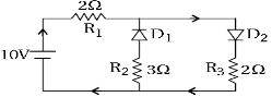
- A
$1.43$
- B
$3.13$
- ✓
$2.5 $
- D
$10$
AnswerCorrect option: C. $2.5 $
c
Diode $D_{1}$ is reverse biased so, it will block the current and diode $D_{2}$ is forward biased, so it will pass the current.
Hence, equivalent circuit becomes as shown in the figure.
Current in the circuit $=$ Current flowing through the resistance
$R_{1}=\frac{10}{2+2}=2.5 \mathrm{A}$
View full question & answer→MCQ 391 Mark
For $CE$ transistor amplifier, the audio signal voltage across the collector resistance of $2 \,\,k\Omega$ is $4\,\, V.$ If the current amplification factor of the transistor is $100$ and the base resistance is $1 \,\,k\Omega$, then the input signal voltage is.......$mV$
Answerd
$\text { Here, } R_{C}=2 \mathrm{k} \Omega=2000 \Omega, V_{0}=4 \mathrm{V}$
$\alpha=100, R_{B}=1 \mathrm{k} \Omega=1000 \Omega, V_{i}=?$
Voltage gain, $A=\beta \frac{R_{C}}{R_{B}}=100 \times \frac{2000}{1000}=200$
$ \text { Also, } A =\frac{V_{0}}{V_{i}} \text { or } V_{i}=\frac{V_{0}}{A}=\frac{4}{200} $
$=\frac{2}{100} \mathrm{V}=20 \mathrm{mV}$
View full question & answer→MCQ 401 Mark
A $npn$ transistor is connected in common emitter configuration in a given amplifier. A load resistance of $800 \,\,\Omega$ is connected in the collector circuit and the voltage drop across it is $0.8\,\, V.$ If the current amplification factor is $0.96$ and the input resistance of the circuit is $192 \,\,\Omega$, the voltage gain and the power gain of the amplifier will respectively be
- A
$3.69,3.84$
- B
$4,4$
- C
$4,3.69$
- ✓
$4,3.84$
AnswerCorrect option: D. $4,3.84$
d
$\text { Here, } R_{0}=800 \Omega, R_{i}=192 \Omega$
current gain, $\beta=0.96$
Voltage gain $=$ Current gain $\times$ Resistance gain
$=0.96 \times \frac{800}{192}=4$
Power gain $=$ [Current gain ] $\times$ [ Voltage gain ]
$=0.96 \times 4=3.84$
View full question & answer→MCQ 411 Mark
What is the output $Y$ in the following circuit, when all the three inputs $A,\, B,\, C$ are first $0$ and then $1$ ?
Answera
$Y=\overline{(A B) C}=\overline{A B C}$
If $A=B=C=0$ then $Y_{0}=\overline{0}=1$
If $A=B=C=0$ then $Y_{1}=\overline{1}=0$
View full question & answer→MCQ 421 Mark
Consider the junction diode as ideal. The value of current flowing through $AB$ is
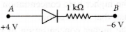
- ✓
$10^{-2}\;A$
- B
$10^{-1}\;A$
- C
$10^{-3}\;A$
- D
$0\;A$
AnswerCorrect option: A. $10^{-2}\;A$
a
Here, the $p-n$ junction diode is forwarc biased, hence it offers zero resistance
$\therefore {{I}_{AB}}=\frac{{{V}_{A}}-{{V}_{B}}}{{{R}_{AB}}}=$ $\frac{4\text{V}-(-6\text{V})}{1\text{k}\Omega }=$ $\frac{10}{1000}\text{A}={{10}^{-2}}\text{A}$
View full question & answer→MCQ 431 Mark
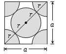
- A
$\frac{a}{2}$
- ✓
$\frac{a}{{2\sqrt 2 }}$
- C
$\frac{{\sqrt 3 }}{4}a$
- D
$\frac{{\sqrt 3 }}{2}a$
AnswerCorrect option: B. $\frac{a}{{2\sqrt 2 }}$
b
(b)For the $ fcc $ structure
$4r = {({a^2} + {a^2})^{1/2}}$$ = a\sqrt 2 $
==> $r = \frac{{a\sqrt 2 }}{4} = \frac{a}{{2\sqrt 2 }}$
View full question & answer→MCQ 441 Mark
The nearest distance between two atoms in case of a $ bcc $ lattice is equal to
- A
$a\frac{{\sqrt 2 }}{3}$
- ✓
$a\frac{{\sqrt 3 }}{2}$
- C
$q\sqrt 3 $
- D
$\frac{a}{{\sqrt 2 }}$
AnswerCorrect option: B. $a\frac{{\sqrt 3 }}{2}$
b
(b)The nearest distance between two atoms in a $bcc$ lattice $= 2$ (atomic radius) $ = 2 \times \left( {\frac{{\sqrt 3 \,a}}{4}} \right) = \frac{{\sqrt 3 a}}{2}$
View full question & answer→MCQ 451 Mark
Sodium has body centred packing. If the distance between two nearest atoms is $3.7 Å,$ then its lattice parameter is.....$Å$
- A
$4.8 $
- ✓
$4.3 $
- C
$3.9 $
- D
$3.3 $
AnswerCorrect option: B. $4.3 $
b
(b)For bcc packing, distance between two nearest atoms $d = 2r = 2\,\left( {\frac{{\sqrt 3 \,a}}{4}} \right)$
==> Lattice constant $a = \frac{{2d}}{{\sqrt 3 }} = \frac{{2 \times 3.7}}{{\sqrt 3 }} = 4.3{Å}$
View full question & answer→MCQ 461 Mark
The energy gap of silicon is $1.14 \ eV$. The maximum wavelength at which silicon will begin absorbing energy is.....$Å$
- ✓
$10888 $
- B
$1088.8 $
- C
$108.88 $
- D
$10.888$
AnswerCorrect option: A. $10888 $
a
(a)${\lambda _{\max }} = \frac{{hc}}{E} = \frac{{6.6 \times {{10}^{ - 34}} \times 3 \times {{10}^8}}}{{1.14 \times 1.6 \times {{10}^{ - 19}}}} = 10888{Å}$
View full question & answer→MCQ 471 Mark
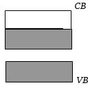
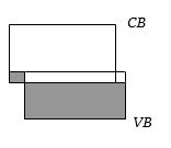
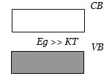
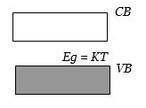
Which of the energy band diagrams shown in the figure corresponds to that of a semiconductor
Answerd
In semiconductors, the forbidden energy gap between the valence band and conduction band is very small, almost equal to $KT.$ Moreover, valence band is completely filled where as conduction band is empty.
View full question & answer→MCQ 481 Mark
Following is the relation between current and charge $I = A{T^2}{e^{qt/{V_L}}}$ then value of $VL$ will be
- A
$\frac{V}{{kT}}$
- B
$\frac{{kV}}{T}$
- ✓
$\frac{{kT}}{V}$
- D
$\frac{{VT}}{k}$
AnswerCorrect option: C. $\frac{{kT}}{V}$
c
(c)Comparing the given equation with standard equation
$i = A{T^2}{e^{qV/kT}}$==> ${V_L} = \frac{{kT}}{V}$.
View full question & answer→MCQ 491 Mark
Which one is correct relation for thermionic emission
- A
$J = A{T^{1/2}}{e^{ - \varphi /kT}}$
- ✓
$J = A{T^2}{e^{ - \varphi /kT}}$
- C
$J = A{T^{3/2}}{e^{ - \varphi /kT}}$
- D
$J = A{T^2}{e^{ - \varphi /2kT}}$
AnswerCorrect option: B. $J = A{T^2}{e^{ - \varphi /kT}}$
View full question & answer→MCQ 501 Mark
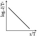
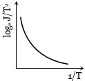
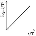
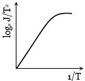
For a thermionic emitter (metallic) if J represents the current density and T is its absolute temperature then the correct curve between ${\log _e}\frac{J}{{{T^2}}}$ and $\frac{1}{T}$ is
Answera
(a)According to Richardson-Dushman equation $J = A{T^2}{e^{ - b/T}}$
Taking log of this equation ${\log _e}\frac{J}{{{T^2}}} = {\log _e}A - \frac{b}{T}$
i.e. graph between ${\log _e}\frac{J}{{{T^2}}}$ and $\frac{1}{T}$ will be a straight line having negative slope and positive intercept $(logeA)$ on ${\log _e}\frac{J}{{{T^2}}}{\rm{axis}}{\rm{.}}$
View full question & answer→