MCQ 11 Mark
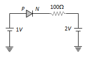
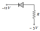
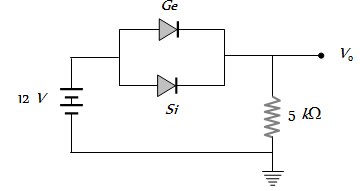
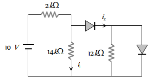
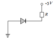
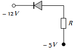
In the following circuit find $I_1$ and $I_2$
- A$ 0, 0$
- B$ 5 mA, 5 mA$
- C$5 mA, 0$
- ✓$0, 5 mA$
Answer
View full question & answer→Correct option: D.
$0, 5 mA$
$0, 5 mA$
50 questions · timed · auto-graded
 2.
2. 3.
3.  4.
4.  5.
5.
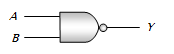
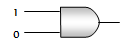
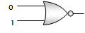
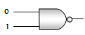
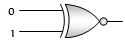
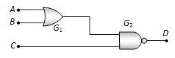
| A | 0 | 0 | 1 | 1 |
| B | 0 | 1 | 0 | 1 |
| X | 0 | 1 | 1 | 1 |